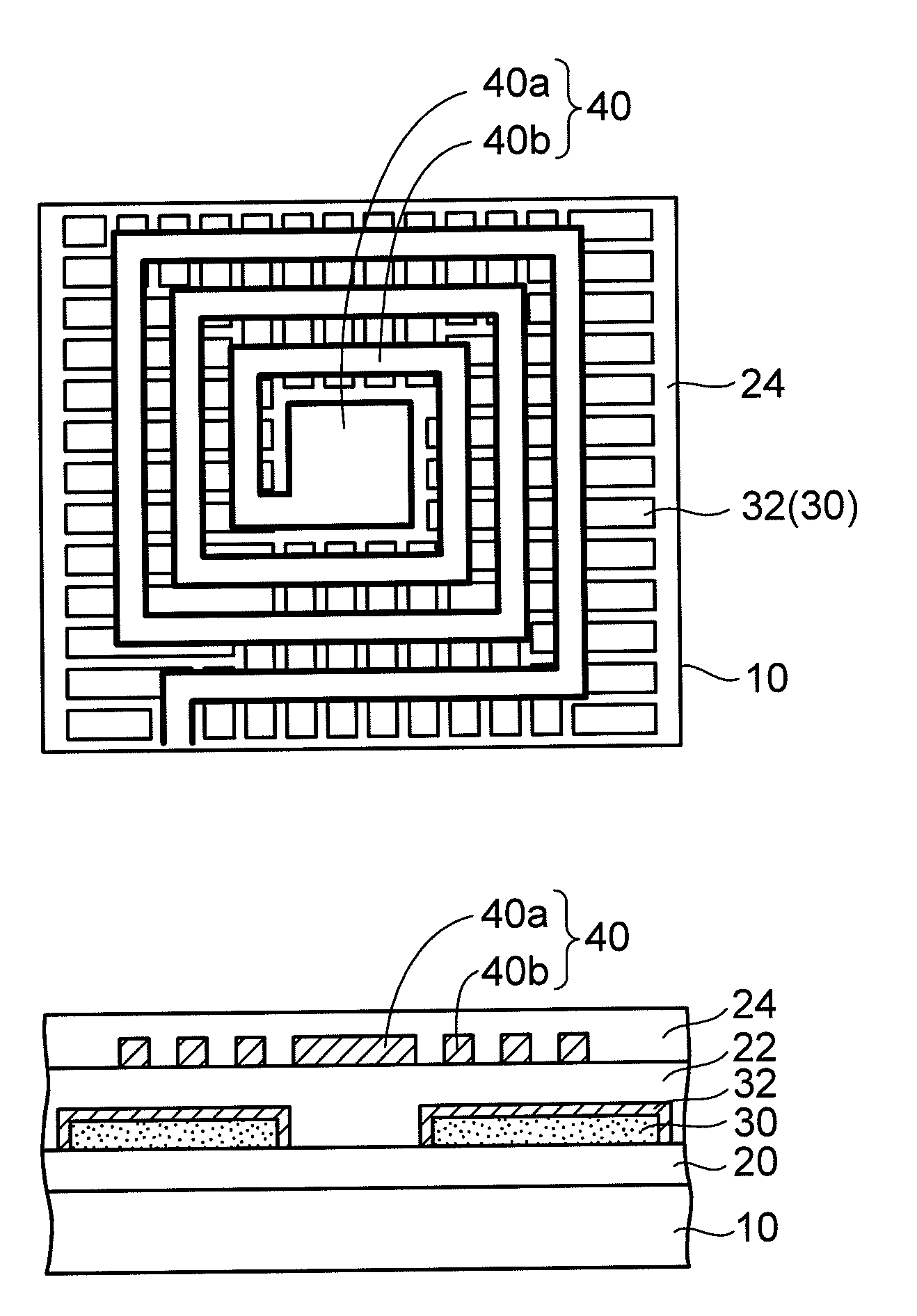
Inductor device, and method of manufacturing the same
a technology of inductor and inductor body, which is applied in the direction of magnets, inductances, magnetic bodies, etc., can solve the problems of increased production costs, increased production costs, and additional costs for designing dedicated components, etc., and achieves high reliability and easy formation
- Summary
- Abstract
- Description
- Claims
- Application Information
AI Technical Summary
Benefits of technology
Problems solved by technology
Method used
Image
Examples
first embodiment
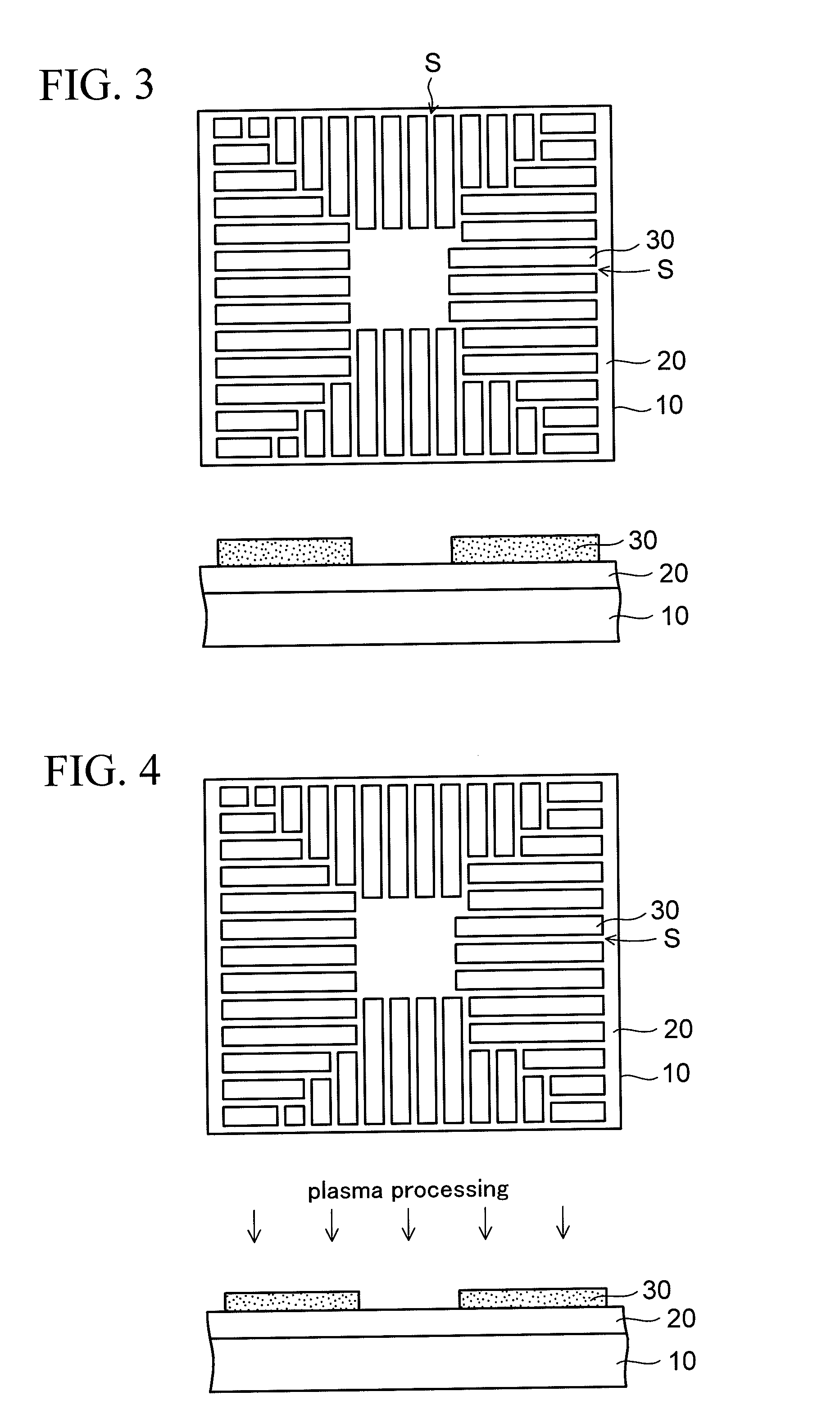
[0038]FIG. 1 to FIG. 12 are plan views and sectional views showing a method of manufacturing an inductor device according to a first embodiment of the present invention respectively. In FIG. 1 to FIG. 12, upper views are a plan view respectively, and lower views are a sectional view respectively.
[0039]In the method of manufacturing the inductor device in the first embodiment, as shown in FIG. 1, first, a first insulating layer 20 is formed on a substrate 10. The first insulating layer 20 is formed of an epoxy resin or a polyimide resin, and that thickness is set to 20 to 200 μm. The first insulating layer 20 is formed by either pasting a resin film on the substrate 10 or coating a liquid resin on the substrate 10.
[0040]Preferably the substrate 10 is the wiring substrate having the wiring layer. As described later, the inductor element connected to the wiring layer is built-in over the substrate 10.
[0041]Then, as shown in FIG. 2, a photosensitive catalyst metal-containing resin layer...
second embodiment
[0093]FIGS. 13A to 13D, FIGS. 14A and 14B, FIG. 15, and FIG. 16 are sectional views showing a method of manufacturing an inductor device according to a second embodiment of the present invention respectively. A feature of the second embodiment resides in that the first and second Ni Co pattern layers arranged to the upper and lower side are brought partially close to each other by providing the holes in the insulating layer, thereby a magnetic coupling is increased.
[0094]In the method of manufacturing the inductor device in the second embodiment, as shown in FIG. 13A, first, an insulating substrate 50 (intermediate insulating layer) whose thickness is 100 to 150 μm is prepared. Then, a through hole TH which penetrates to the thickness direction is formed in the insulating substrate 50 by the drilling, or the like.
[0095]Then, as shown in FIG. 13B, the first and second planar coil layers 40, 42 made of copper, or the like are formed on both surface sides of the insulating substrate 50...
PUM
| Property | Measurement | Unit |
|---|---|---|
| Shape | aaaaa | aaaaa |
| Area | aaaaa | aaaaa |
| Magnetism | aaaaa | aaaaa |
Abstract
Description
Claims
Application Information
 - R&D
- Intellectual Property
- Life Sciences
- Materials
- Tech Scout
- Unparalleled Data Quality
- Higher Quality Content
- 60% Fewer Hallucinations
Browse by: Latest US Patents, China's latest patents, Technical Efficacy Thesaurus, Application Domain, Technology Topic, Popular Technical Reports.
© 2025 PatSnap. All rights reserved.Legal|Privacy policy|Modern Slavery Act Transparency Statement|Sitemap|About US| Contact US: help@patsnap.com


