
Tamper-detecting electronic system

Active Publication Date: 2010-07-22
CISCO TECH INC
View PDF9 Cites 29 Cited by
  • Summary
  • Abstract
  • Description
  • Claims
  • Application Information

AI Technical Summary

Benefits of technology

[0079]Moreover in accordance with an embodiment of the present invention, enabling the IC to control the strength of said electrical current of known strength.

Problems solved by technology

In this fashion the crackers can more easily study and reverse engineer operating security chips, thereby greatly compromising the security of the security chips.
Most such known protection methods are easily circumventable by those skilled in the art of cracking.

Method used


Image

  • Tamper-detecting electronic system
  • Tamper-detecting electronic system
  • Tamper-detecting electronic system

Examples


Embodiment Construction

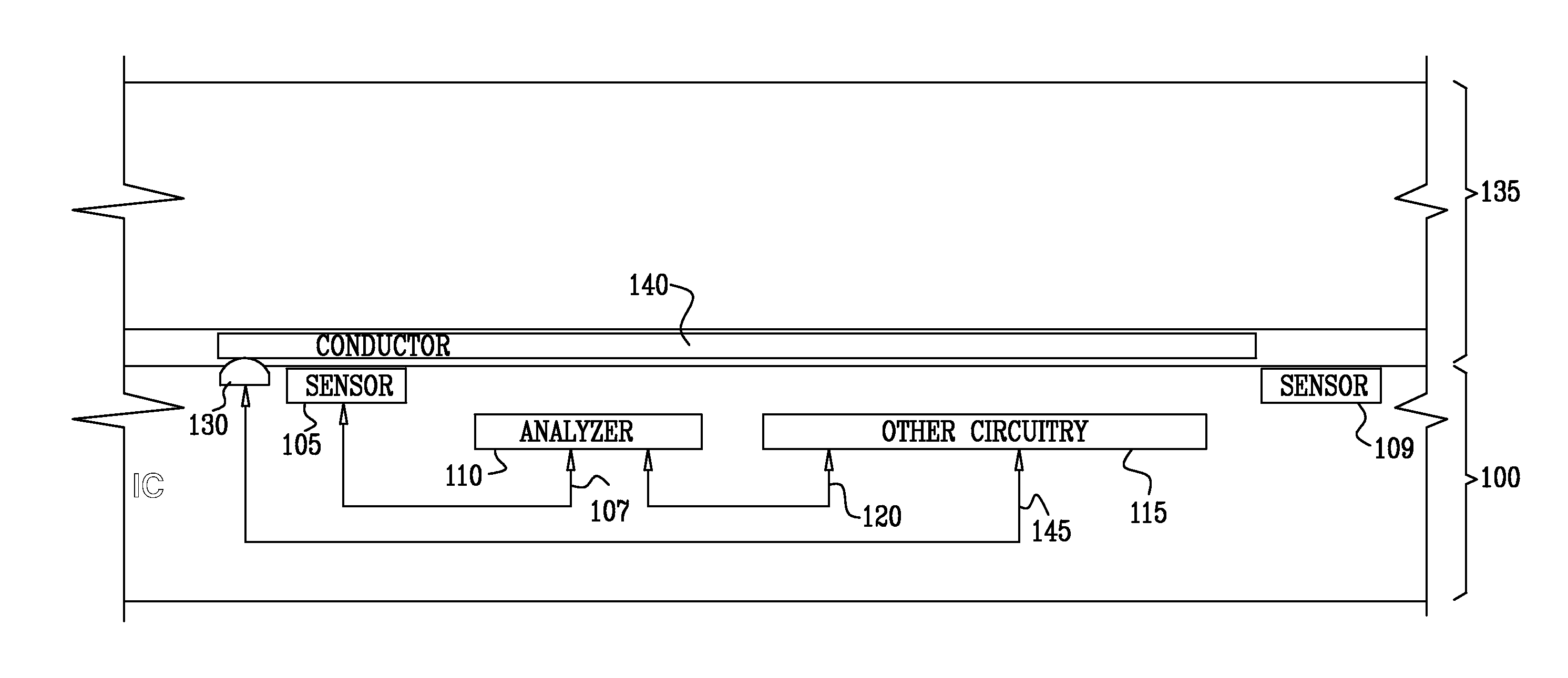
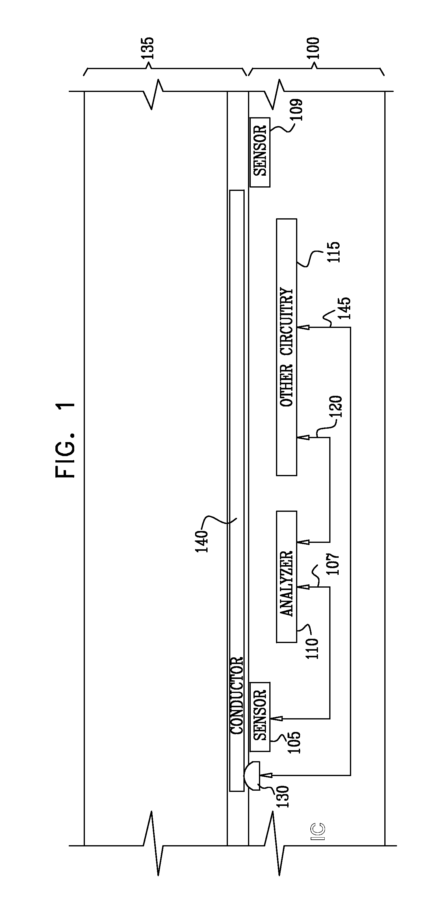
[0135]Reference is now made to FIG. 1, which is a schematic cross-sectional illustration of an integrated circuit (IC) 100 constructed and operative in accordance with an embodiment of the present invention, the IC being in operative electrical association with a second circuit 135.

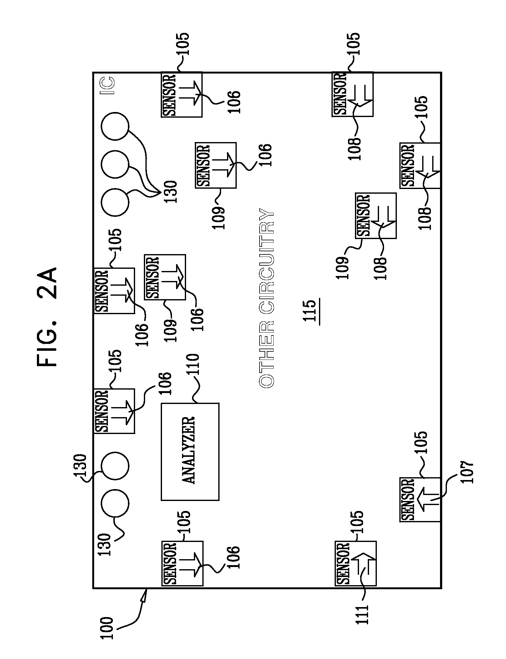
[0136]The apparatus of FIG. 1 comprises an IC 100 and a second circuit 135. The IC 100, of the present example, comprises at least one magnetic field sensing device 105, a background magnetic field sensing device 109, an analyzer 110, and other circuitry 115.

[0137]The analyzer 110 is in operative association, via an electrically conducting connection 107, with the at least one magnetic field sensing device 105.

[0138]The other circuitry 115 is in operative association with the analyzer 110 via an electrically conducting connection 120.

[0139]The apparatus of FIG. 1 additionally comprises a second circuit 135 not comprised in the IC 100. In an embodiment of the invention, the second circuit 135 is in operati...


PUM


Abstract

An apparatus for detecting tampering with an integrated circuit (IC), the apparatus comprising a second circuit comprising at least one conductor for conducting electrical current, the electrical current comprising, during at least one period of time, current of known strength, the electrical current generating a magnetic field, at least one magnetic field sensing device operatively associated with the IC, the sensing device having at least one electrical characteristic responsive to changes in a sensed magnetic field, the magnetic field sensing device being positioned so as to sense the magnetic field generated by current in the at least one conductor, and an analyzer operatively associated with the at least one magnetic field sensing device and the IC, the analyzer determining that the IC is being tampered with based, at least in part, on changes in the at least one electrical characteristic of the at least one magnetic field sensing device in response to changes in the sensed magnetic field generated by the electrical current in the at least one conductor during the at least one period of time. Related apparatus and methods are also described.

Description

FIELD OF THE INVENTION[0001]The present invention relates to electronic systems which comprise electronic sub-systems designed to detect tampering with the electronic systems.BACKGROUND OF THE INVENTION[0002]Security integrated circuits, commonly known as “security chips”, are often used to protect information, data transmissions, access control, or value (typically monetary). Data in security chips is typically protected through the use of secure memory and / or the secure transmission of data using cryptographic techniques implemented on chip. Some applications for security chips include: banking cards, television conditional access system cards, premises access control cards, personal identity cards, USB flash drives and automobile keys.[0003]“Crackers”, people who use their expertise to illegally break into secure programs and systems, have been known to remove security chips from their packaging and then to connect the security chips to suitable electrical connections in such a w...

Claims


Application Information

Patent Timeline
IPC IPC(8): G01R33/12G06F21/86
CPCG06F21/86
Inventor SUDAI, RAMISHLOMOVICH, YONATANKATZ, SAMUEL
Owner CISCO TECH INC
Learn More