
LED illumination device using diffraction member

a technology of led illumination and diffraction member, which is applied in the direction of semiconductor devices, lighting and heating apparatus, instruments, etc., can solve the problems of reducing the luminous efficiency of conventional led, reducing the efficiency of transmitting light outside, and reducing the efficiency of enlarging the area, so as to reduce the loss of luminous intensity at the light diffusion member, uniform light, and lessen the degree of light diffusing

Inactive Publication Date: 2010-07-22
ABEL SYST
View PDF1 Cites 8 Cited by
  • Summary
  • Abstract
  • Description
  • Claims
  • Application Information

AI Technical Summary

Benefits of technology

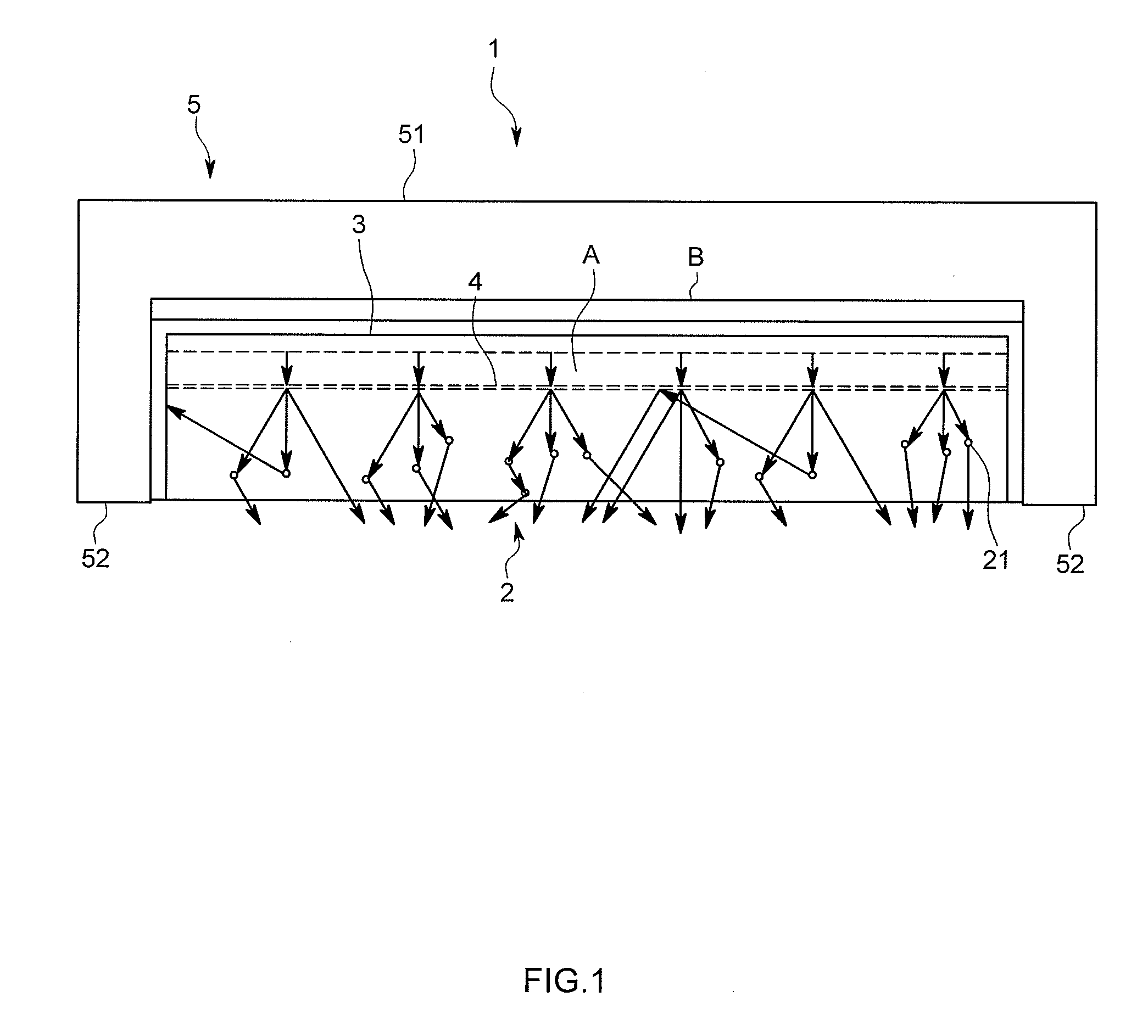
[0020]In accordance with this invention having the above arrangement, since the diffraction member is arranged between the LED and the diffusion member, it is possible to obtain more uniform light compared to a case where the light is diffused by the light diffusion material alone. In addition, in the case of obtaining the light having the same uniform degree, since it is possible for the LED illumination device having the light diffraction sheet to lessen the light diffusing degree at the light diffusion member compared to the LED illumination device having the light diffusion member alone, a loss of luminous intensity at the light diffusion member can be reduced, thereby improving the efficiency as a whole.
[0021]Furthermore, since it is possible to conduct the ideal plane emission and to bring a large amount of the light intensity of the generated light to outside with high efficiency by making use of the dielectric antennas, it is possible not only to secure a light intensity necessary for a general illumination device but also to reduce the generation of heat because of the high efficiency. As a result, a resin having a small heat resistance can be used for the diffraction member or the diffusion member, a freedom degree in designing a shape or a material of the diffraction member or the diffusion member can be greatly enlarged, which makes it possible to provide the most appropriate illumination device appropriate for various purposes.

Problems solved by technology

One of these causes is that the conventional LED is low in luminous efficiency and small in luminous area.
However, since an electrode is attached to the surface of the semiconductor element and the electrode blocks the light, it impedes the improvement of the efficiency of transmitting the light outside and impedes increasing the light intensity by enlarging the area.
In spite of this, if the area of the electrode is made small, more than a certain level in comparison with the area of the semiconductor element, it becomes impossible to provide a uniform electric field to the entire semiconductor element, thereby declining the luminescent amount.
As a result, even though the area of the semiconductor element is enlarged in order to obtain a large amount of the light intensity, there is no other choice but to enlarge the area of the electrode in order to enable the plane emission, which makes it difficult to take a large amount of the light intensity outside because of the light shielding effect.
In addition, in view of the problem it is conceived that a transparent electrode such as an ITO is used, however, since a specific resistance of the transparent electrode is bigger in comparison with that of a metal electrode, a loss is generated at the metal electrode so that the luminous efficiency is lowered.

Method used


Image

  • LED illumination device using diffraction member
  • LED illumination device using diffraction member
  • LED illumination device using diffraction member

Examples


Embodiment Construction

[0030]Embodiments of this invention will be explained with reference to FIG. 1 through FIG. 8.

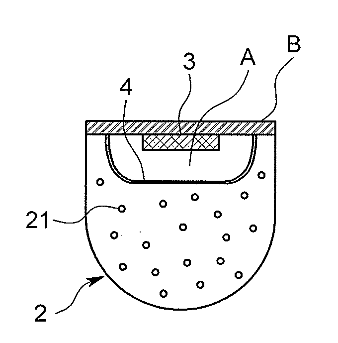
[0031]An LED illumination device 1 in accordance with this embodiment is used for general lighting such as a room lighting instead of, for example, a fluorescent lamp, and comprises, as shown in FIG. 1, a diffusion member 2, an LED 3 mounted on the diffusion member 2, a light diffraction sheet 4 mounted on the diffusion member 2, and a holding body 5 that holds the diffusion member 2, the LED 3 and the light diffraction sheet 4.

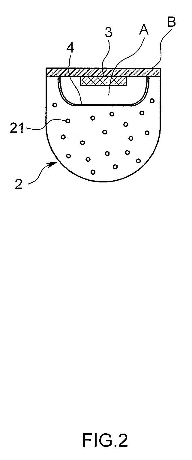
[0032]The diffusion member 2 is transparent and made of resin and contains light scattering particles 21 to diffuse the light inside. A shape of the diffusion member 2 is, for example, a column whose cross-section is generally a half circle as shown in FIG. 1 and FIG. 2. In this embodiment, a groove (A) is arranged to extend in a longitudinal direction at a string side of the generally half circle in the cross sectional view. Furthermore, a board (B) is arranged to c...


PUM


Abstract

An object of this invention is to provide an LED illumination device that can substitute for a fluorescent light and obtain uniform light with high efficiency. The LED illumination device comprises an LED with a thin-plate-shaped semiconductor element body transmitting the light generated in a PN junction area in a thickness direction and emits it from the surface, a surface electrode that covers the surface of the semiconductor element body, and columnar dielectric antennas that penetrate the surface electrode in the thickness direction and that condense the light transmitted in a body of the semiconductor element and emit it outside, a diffraction member that is arranged on a luminous surface side of the LED and that diffracts and disperses the light emitted by the LED, and a diffusion member that is arranged outside the diffraction member and that diffuses the light dispersed by the diffraction member and emits it outside.

Description

FIELD OF THE ART[0001]This invention relates to an LED illumination device using a high efficiency LED that can produce plane emission.BACKGROUND ART[0002]Since an LED has a longer operating life and its light intensity is more stable compared to a fluorescent light or an incandescent lamp, no time is required for starting-up the LED and there is no problem of discarding the LED. Recently a high power LED was developed in addition to the LED that emits blue light or ultraviolet light so that applications of LEDs are expanding not only to include conventional indicators but also to include general illumination devices.[0003]However, in view of a total light intensity or an illumination intensity, even though a light intensity per unit illuminating area is increasing, the LED is still behind the fluorescent light. In order to obtain a light intensity comparable to that of the fluorescent light in total, a lot of LEDs are required and a heat release value also gets very big, which requ...

Claims


Application Information

Patent Timeline
Patent Type & Authority Applications(United States)
IPC IPC(8): H01L33/00H01L33/20H01L33/38H01L33/50
CPCF21K9/00G02B5/02G02B5/1809F21Y2103/003H01L33/382H01L33/508F21K9/30H01L33/20F21K9/20F21Y2103/10F21Y2115/10
Inventor SUZUKI, FUMIO
Owner ABEL SYST
Learn More