Method for preventing data loss during solder reflow process and memory device using the same
- Summary
- Abstract
- Description
- Claims
- Application Information
AI Technical Summary
Benefits of technology
Problems solved by technology
Method used
Image
Examples
Embodiment Construction
[0017]The following description is of the best-contemplated mode of carrying out the invention. This description is made for the purpose of illustrating the general principles of the invention and should not be taken in a limiting sense. The scope of the invention is best determined by reference to the appended claims.
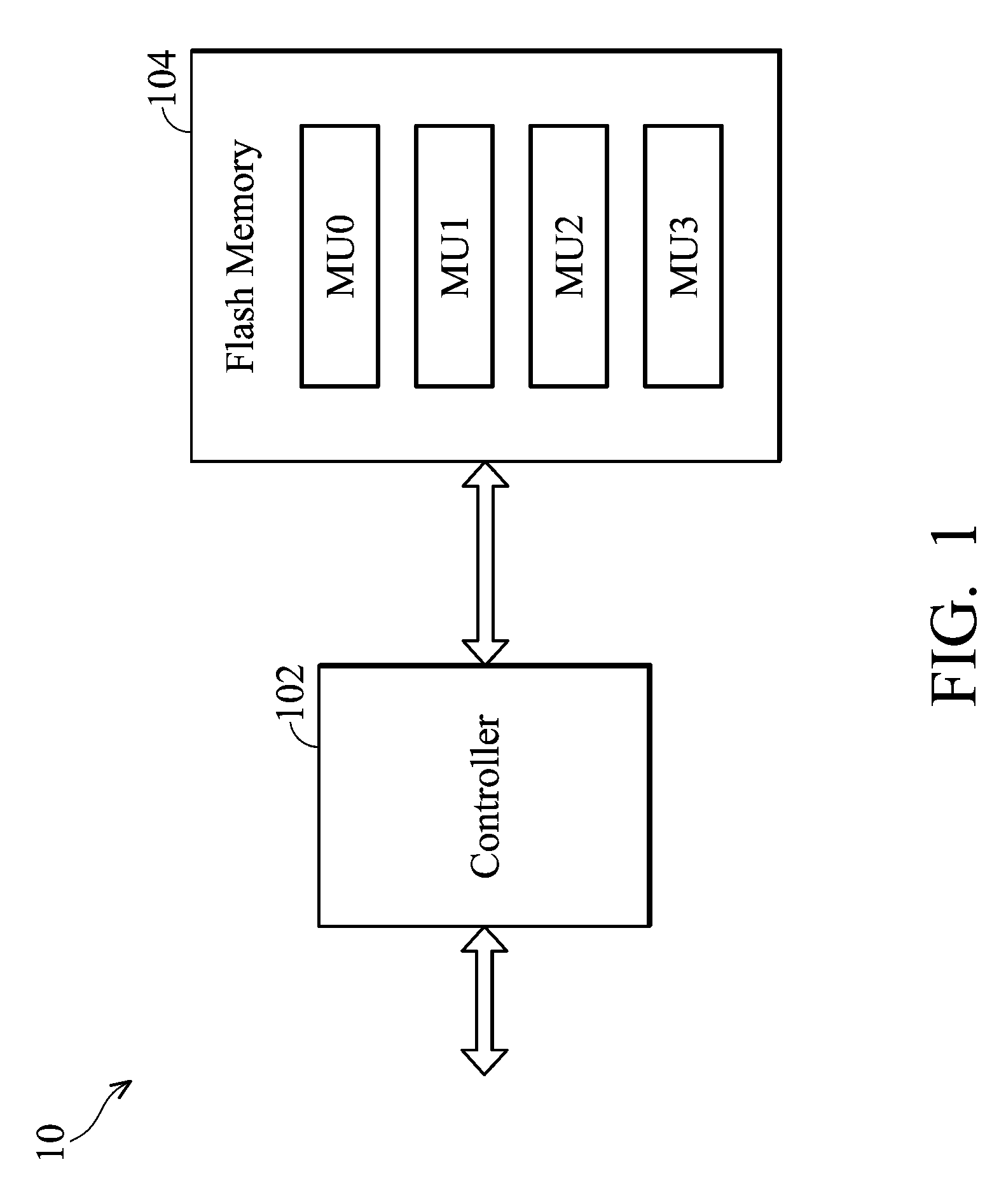
[0018]FIG. 1 is a block diagram of a memory device 10 according to an embodiment of the invention. The memory device 10 comprises a flash memory 104 and a controller 102.
[0019]In an embodiment, the memory device 10 is a memory card or a solid state disk (SSD). The flash memory 104 is a NAND flash memory. The memory device 10 transmits and receives data to an external host (not shown in FIG. 1), e.g., a digital camera or a cell phone, via different interfaces, such as a universal serial bus (USB), a personal computer memory card international association (PCMCIA), or a serial advanced technology attachment (SATA).
[0020]During operation, the controller 102 is coupled bet...
PUM
 Abstract
Description
Claims
Application Information
 - R&D
- Intellectual Property
- Life Sciences
- Materials
- Tech Scout
- Unparalleled Data Quality
- Higher Quality Content
- 60% Fewer Hallucinations
Browse by: Latest US Patents, China's latest patents, Technical Efficacy Thesaurus, Application Domain, Technology Topic, Popular Technical Reports.
© 2025 PatSnap. All rights reserved.Legal|Privacy policy|Modern Slavery Act Transparency Statement|Sitemap|About US| Contact US: help@patsnap.com


