LED module and packaging method thereof
a technology of led modules and led lamps, applied in semiconductor/solid-state device testing/measurement, instruments, light support devices, etc., can solve the problems of low popularity of led lamps, use of light control elements, and high cos
- Summary
- Abstract
- Description
- Claims
- Application Information
AI Technical Summary
Benefits of technology
Problems solved by technology
Method used
Image
Examples
first embodiment
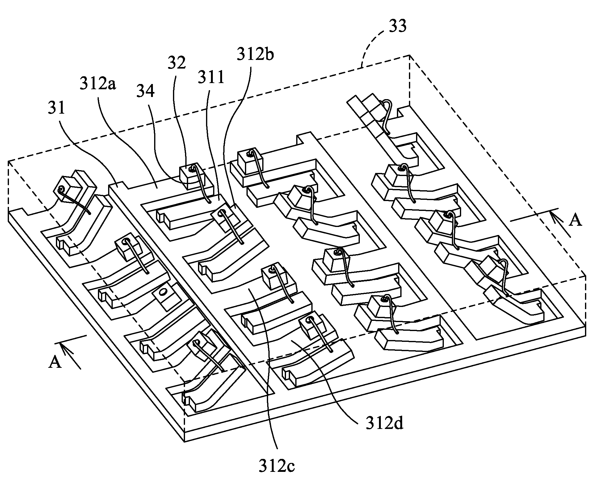
[0035]Please refer to FIG. 4, which is a cross-sectional diagram of a packaging structure for an LED module according to the disclosure. The LED module 1 comprises a plurality of lead frames 11, each being bended by a predetermined angle according to a candela distribution curve to construct a tilted plane 112; and a plurality of LED chips 12, each being fixedly disposed on the tilted plane 112 constructed by each of the lead frames 11. The lead frames 11 comprise Cu, Fe, Ni or combination thereof. The LED chips 12 comprise semiconductor materials such as GaN, GaInN, AlInGaP, AlInGaN, AlN, InN, GaInAsN and GaInPN. The LED chips 12 are sapphire-based, thin-GaN LED's or flip-chip packaged. Moreover, each of the lead frames 11 is provided with a heat sink 14 at the bottom. The lead frames 11, LED chips 12 and the heat sink 14 are further covered by a transparent encapsulant 13.
second embodiment
[0036]Please refer to FIG. 5A, which is a cross-sectional diagram of a packaging structure for an LED module according to the disclosure. FIG. 5A is different from FIG. 4 in that the tilted plane 112 is recessed to form a cup 111 having a reflective surface so that the light from the LED chip 12 is more uniform than in FIG. 4.
[0037]FIG. 5B is a cross-sectional diagram of a packaging structure for an LED module according to a third embodiment of the disclosure; and FIG. 5C is a three-dimensional diagram of a packaging structure for an LED module according to a fourth embodiment of the disclosure. In FIG. 5B and FIG. 5C, a cup 113 having a reflective surface protrudes from the tilted plane 112 so that the light from the LED chip 12 is more uniform. The cup 113 can be formed by injection molding.
[0038]Please refer to FIG. 6, which is a flowchart of a LED packaging method according to a first embodiment of the disclosure. Meanwhile, please refer to FIG. 7 for a cross-sectional diagram o...
PUM
 Abstract
Description
Claims
Application Information
 - R&D
- Intellectual Property
- Life Sciences
- Materials
- Tech Scout
- Unparalleled Data Quality
- Higher Quality Content
- 60% Fewer Hallucinations
Browse by: Latest US Patents, China's latest patents, Technical Efficacy Thesaurus, Application Domain, Technology Topic, Popular Technical Reports.
© 2025 PatSnap. All rights reserved.Legal|Privacy policy|Modern Slavery Act Transparency Statement|Sitemap|About US| Contact US: help@patsnap.com


