
Pixel array with shared readout circuitry

a readout circuit and array technology, applied in the field of pixel arrays, can solve the problems of non-reset of all pixels in a row, non-correctable defect lines of pixels, and high speed and/or lower power consumption, so as to reduce the capacitance of the control line/column bus, reduce the overall readout circuitry, and improve the effect of power consumption and electro-optical performan

Active Publication Date: 2010-06-17
CMOSIS
View PDF35 Cites 23 Cited by
  • Summary
  • Abstract
  • Description
  • Claims
  • Application Information

AI Technical Summary

Benefits of technology

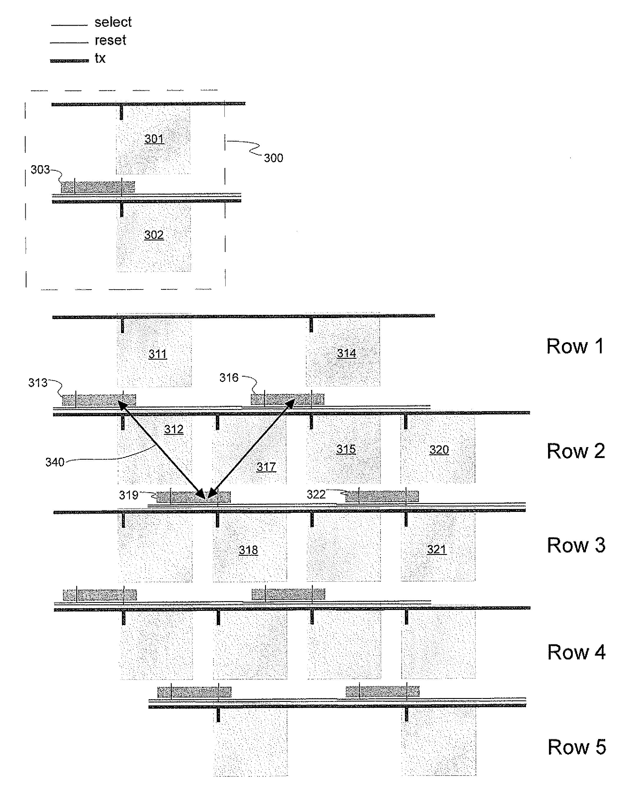
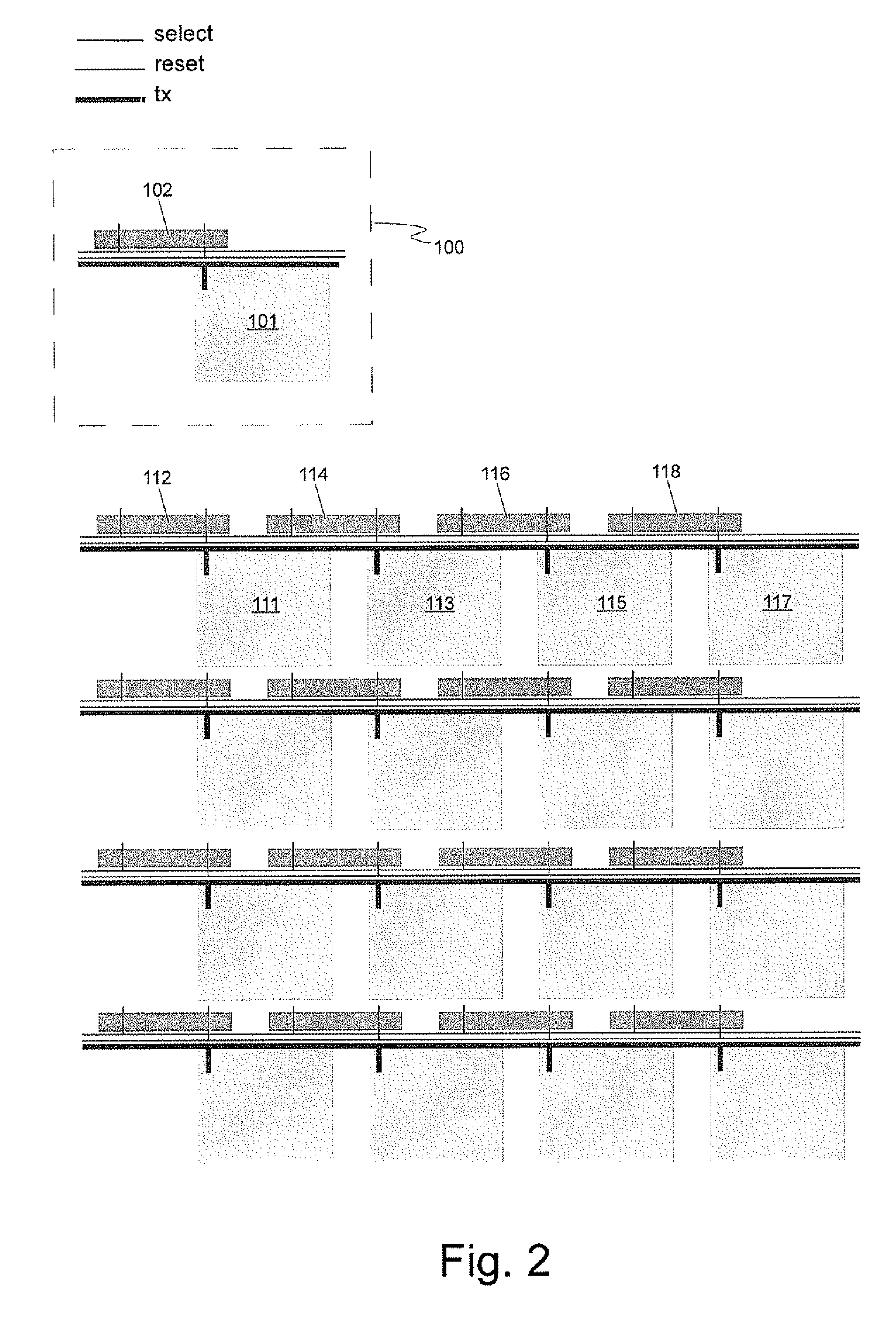
[0011]Advantageously, each repetition of the unit block / readout circuitry is offset by a horizontal distance of one column and by a vertical distance of one row from the nearest adjacent instance of the unit block. A pixel array with shared readout circuitry has some advantages in terms of speed, power consumption and electro-optical performance compared to an array of non-shared pixels. Sharing readout circuitry between photo-sensitive elements requires less overall readout circuitry, and this in turn lowers the capacitance of the control lines / column bus. This leads to higher speed and / or lower power consumption. Less circuitry in the pixels leaves more area for the photo-sensitive elements, which can increase the full well charge of the pixels. Less control lines improves the fill factor of pixels as there are fewer metal tracks blocking the incident light.
[0012]Shared pixel layouts conventionally require approximately one half of the interconnect lines of non-shared pixels, and are therefore expected to have better yields (e.g. in terms of shorts between metal lines since less interconnect lines are vulnerable to defects). However, the traditional sharing approach is susceptible to single defect lines, and a defect line immediately results in a non-correctable defect line of pixels. For example, if a reset line which controls a row of pixels has a defect in the form of a short to ground, all of the pixels in that row cannot be reset. In contrast, the staggered layout has an advantage that a defect in a control line will affect only half of the pixels in a row, as the other pixels in that row will be served by a different control line.

Problems solved by technology

This leads to higher speed and / or lower power consumption.
However, the traditional sharing approach is susceptible to single defect lines, and a defect line immediately results in a non-correctable defect line of pixels.
For example, if a reset line which controls a row of pixels has a defect in the form of a short to ground, all of the pixels in that row cannot be reset.

Method used


Image

  • Pixel array with shared readout circuitry
  • Pixel array with shared readout circuitry
  • Pixel array with shared readout circuitry

Examples


Embodiment Construction

[0039]The present invention will be described with respect to particular embodiments and with reference to certain drawings but the invention is not limited thereto but only by the claims. The drawings described are only schematic and are non-limiting. In the drawings, the size of some of the elements may be exaggerated and not drawn on scale for illustrative purposes. Where the term “comprising” is used in the present description and claims, it does not exclude other elements or steps. Furthermore, the terms first, second, third and the like in the description and in the claims, are used for distinguishing between similar elements and not necessarily for describing a sequential or chronological order. It is to be understood that the terms so used are interchangeable under appropriate circumstances and that the embodiments of the invention described herein are capable of operation in other sequences than described or illustrated herein.

[0040]FIG. 5 shows a pixel architecture with sh...


PUM


Abstract

A pixel array comprises a plurality of photo-sensitive elements arranged in rows and columns and readout circuitry for reading a value of a photo-sensitive element. Shared readout circuitry is provided for a pair of adjacent photo-sensitive elements. Adjacent instances of the shared readout circuitry are staggered with respect to one another. For a layout having shared readout circuitry for a pair of photo-sensitive elements, adjacent instances of the shared readout circuitry are offset by a horizontal distance of one column and a vertical distance of one row of the array. The shared readout circuitry can serve a pair of adjacent photo-sensitive elements in a row or column of the array, or a pair of photo-sensitive elements which are diagonally adjacent in the array. An improved yield and symmetry results from staggering instances of the shared readout circuitry.

Description

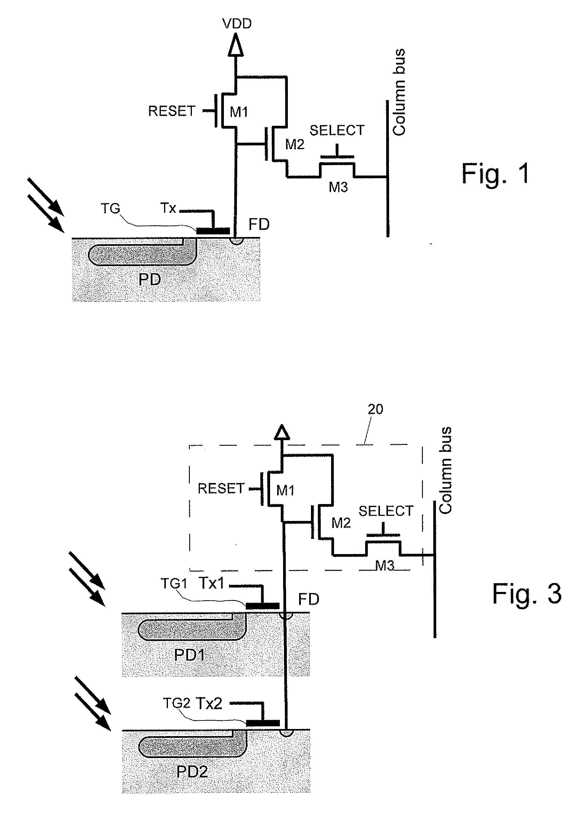
FIELD OF THE INVENTION[0001]This invention relates to pixel arrays which can be used in applications such as image sensors.BACKGROUND TO THE INVENTION[0002]FIG. 1 shows a schematic of a typical pinned photodiode four transistor (4T) active pixel, of the type used in image sensors. The active pixel comprises a pinned photodiode PD, a transfer gate TG, a reset transistor M1, a buffer amplifier M2 and a select transistor M3. A pinned photodiode PD is selectively connected to a sense node FD via the transfer gate TG. The transfer gate TG is controlled by a control line Tx. The reset transistor M1 connects between the sense node FD and a supply line VDD. Transistor M1 is controlled by a signal RESET. Transistor M2 is also connected to the sense node FD and is configured as a source-follower amplifier which acts as a buffer amplifier for the signal generated by the photodiode PD. A transistor M3 connects between the output of the buffer amplifier M2 and an output bus and is controlled by ...

Claims


Application Information

Patent Timeline
IPC IPC(8): H03K17/78H03F3/08H04N5/347H04N5/365H04N5/367H04N5/3745
CPCH01L27/14603H01L27/14621H04N5/347H01L27/14641H04N5/367H04N5/3745H04N5/3651H04N25/46H04N25/671H04N25/68H04N25/77H04N3/15H01L27/14609H01L27/14643H04N25/00
Inventor BOGAERTS, JANMEYNANTS, GUY
Owner CMOSIS
Learn More