
Light emitting element

a technology of light emitting elements and convex parts, which is applied in the direction of basic electric elements, electrical apparatus, and semiconductor devices, etc., can solve the problems of concave and convex portions breaking, and achieve the effect of suppressing cracks or broken, not lowering the light extraction efficiency of the light emitting device, and reducing the stress of convex portions

Inactive Publication Date: 2010-05-13
HITACHI CABLE
View PDF4 Cites 23 Cited by
  • Summary
  • Abstract
  • Description
  • Claims
  • Application Information

AI Technical Summary

Benefits of technology

[0013]an embedded part for transmitting a light emitted from the active layer and reducing stress generated in the plurality of convex portions, the embedded part being formed between two adjacent convex portions of the plurality of convex portions.
[0023]According one embodiment of the invention, a light emitting element is constructed such that plural convex portions are formed on the light extraction surface, a concave portion formed between two adjacent ones is embedded with a material with a linear expansion coefficient close to that of a semiconductor material composing the convex portions. Thereby, even when thermal shock is applied to a light emitting device produced by sealing the light emitting element with a resin, stress occurred in the convex portions can be reduced. Thus, the convex portions are suppressed from being cracked or broken so as not to lower the light extraction efficiency of the light emitting device.

Problems solved by technology

However, in case of the light emitting element described in Patent Literature 1, if silicon is embedded in the textured surface for enhancing a light extraction efficiency, namely, a surface having concave and convex portions, a breaking may occur in the concave and convex portions due to a thermal shock applied to the light emitting element.

Method used


Image

  • Light emitting element
  • Light emitting element
  • Light emitting element

Examples


first embodiment

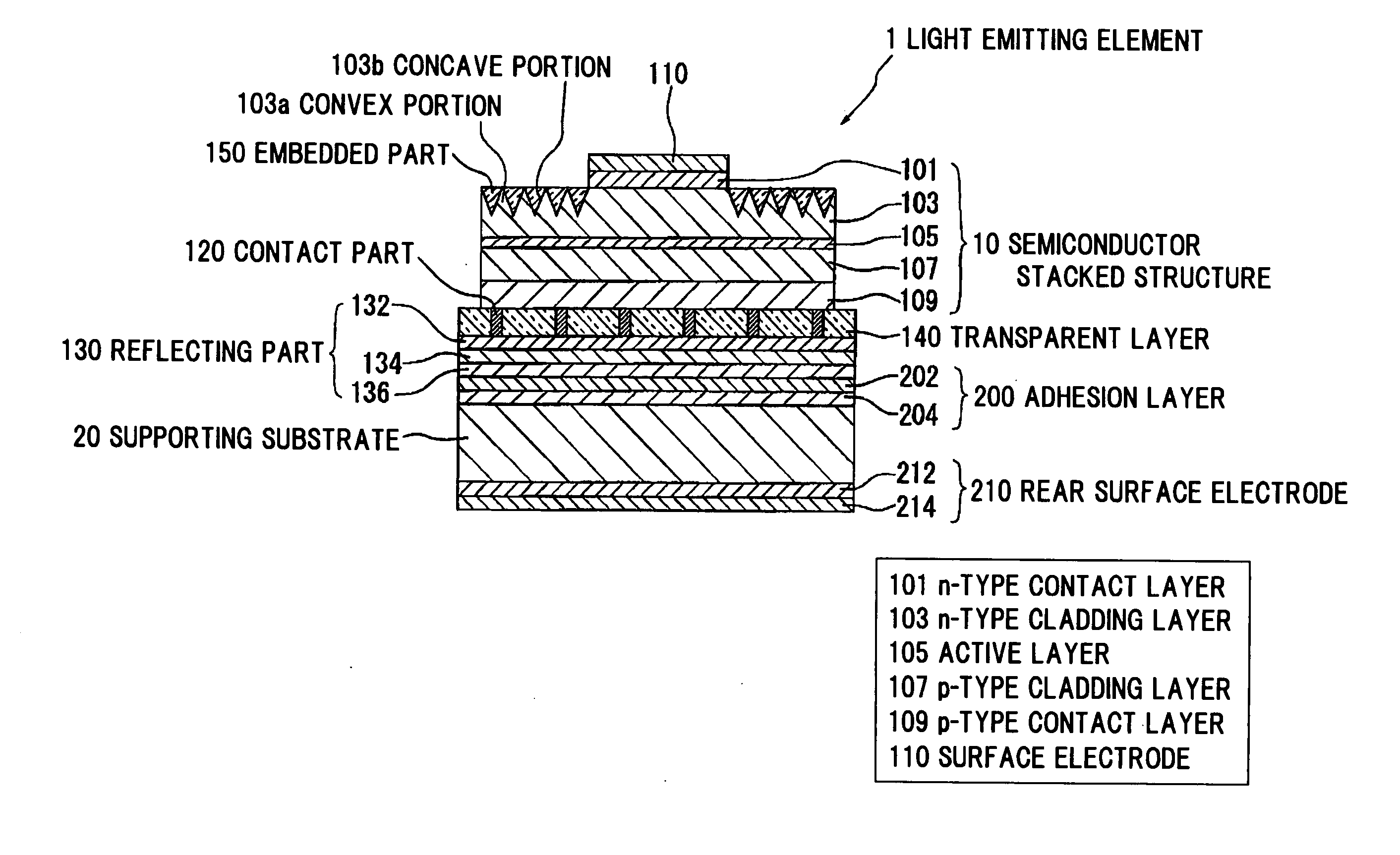
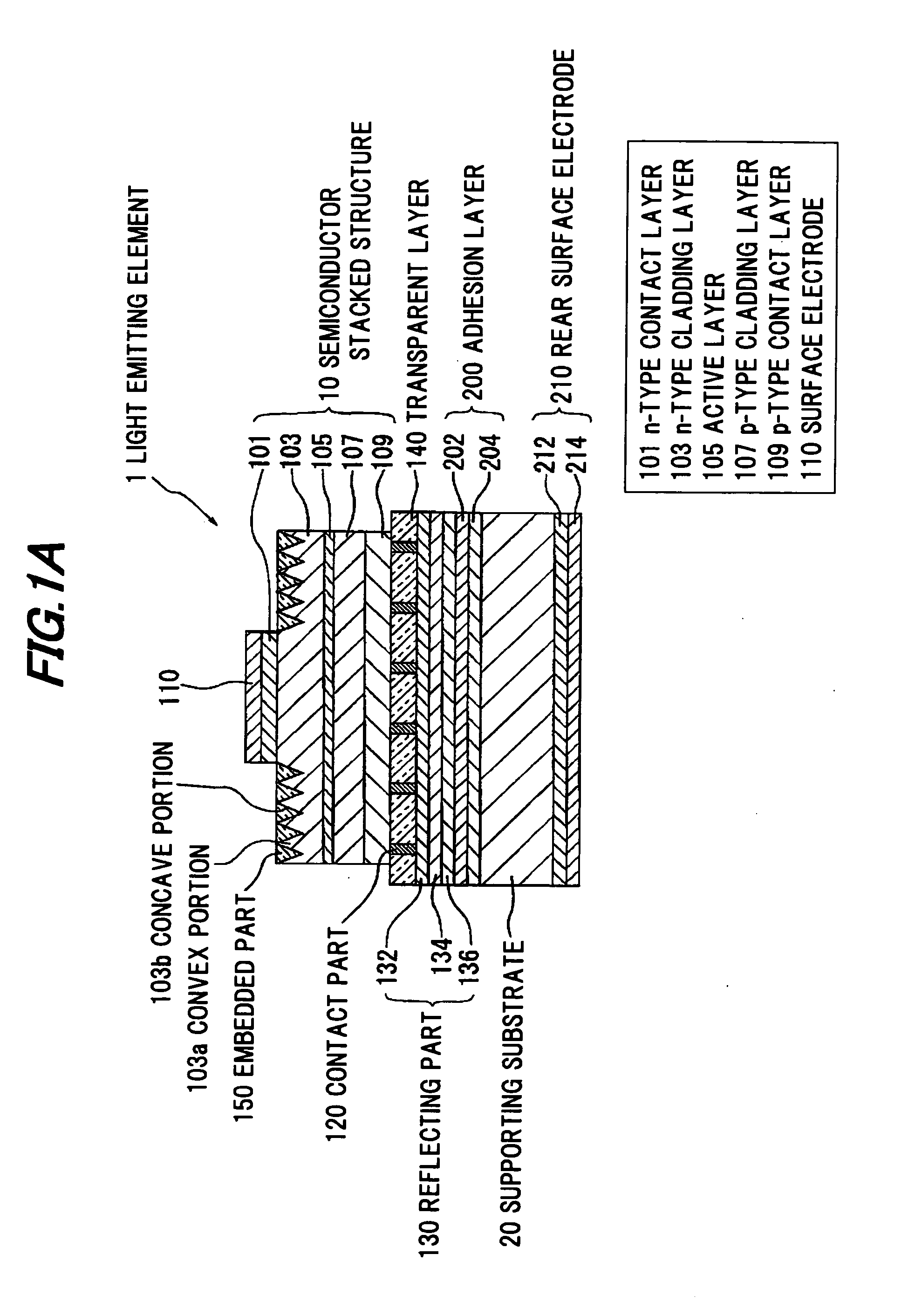
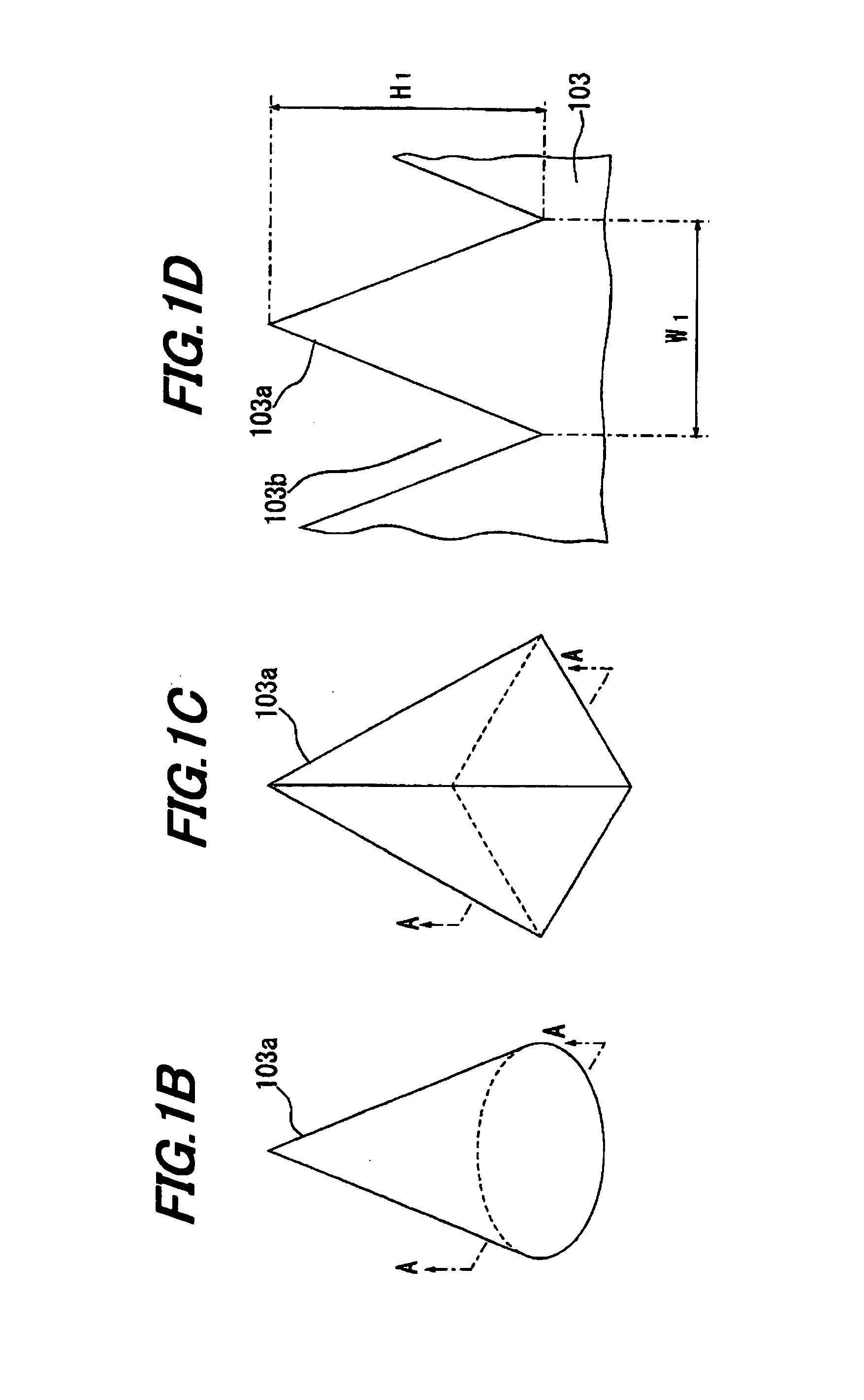
[0036]FIG. 1A is a schematic cross-sectional view showing a light emitting element in a first embodiment according to the invention. FIGS. 1B and 1C are schematic perspective views showing convex portions in the first embodiment according to the invention, and FIG. 1D is a cross-sectional view cut along the line A-A in FIGS. 1B and 1C.

[0037]Schematic Structure of Light Emitting Element 1

[0038]Referring to FIG. 1A, the light emitting element 1 according to the first embodiment includes a semiconductor stacked structure 10 including an active layer 105 for emitting a light having a predetermined wavelength, a surface electrode 110 electrically connected to a partial region of one surface of the semiconductor stacked structure 10, a contact part 120 brought into ohmic contact with a partial region of another surface of the semiconductor stacked structure 10, a transparent layer 140 disposed so as to contact the another surface of the semiconductor stacked structure 10 excluding a regio...

second embodiment

[0111]FIG. 5 is a schematic cross-sectional view showing a part of a light emitting element in a second preferred embodiment according to the invention.

[0112]The light emitting element 2 of the second embodiment has the same composition as the light emitting element 1 of the first embodiment except that the thickness of the embedded part 150 is different. Thus, the detailed explanation of the components except the different components will be omitted below.

[0113]The light emitting element 2 of the second embodiment is constructed such that the embedded part 150 is formed to cover the tip portion of the convex portion 103a as well as the inside of the concave portion 103b. Namely, the embedded part 150 of the second embodiment is formed to have a thickness greater than that of the first embodiment. The light emitting element 2 of the second embodiment can also reduce stress occurred in the convex portion 103a since the convex portion 103a is completely enclosed by the embedded part 1...

third embodiment

[0114]FIG. 6 is a schematic cross-sectional view showing a part of a light emitting element in a third preferred embodiment according to the invention.

[0115]The light emitting element 3 of the third embodiment has the same composition as the light emitting element 1 of the first embodiment except that the structure of the embedded part 150 is different. Thus, the detailed explanation of the components except the different components will be omitted below.

[0116]The light emitting element 3 of the third embodiment is provided with the embedded part 150 composed of multiple embedded layers stacked. For example, a first embedded layer 150a is formed on the concave portion 103b, a second embedded layer 150a is formed on the first embedded layer 150a, and a third embedded layer 150c is formed on the first embedded layer 150b. Thus, the embedded part 150 of the third embodiment is composed of the first to third embedded layers 150a to 150c.

[0117]The materials for forming the first to thir...


PUM


Abstract

A light emitting element includes a semiconductor stacked structure including a first semiconductor layer of first conductivity type, a second semiconductor layer of second conductivity type different from the first conductivity type and an active layer sandwiched between the first semiconductor layer and the second semiconductor layer. The light emitting element further includes a plurality of convex portions formed on one surface of the semiconductor stacked structure, and an embedded part for transmitting a light emitted from the active layer and reducing stress generated in the plurality of convex portions, the embedded part being formed between two adjacent convex portions of the plurality of convex portions.

Description

[0001]The present application is based on Japanese patent application No. 2008-287314 filed on Nov. 10, 2008, the entire contents of which are incorporated herein by reference.BACKGROUND OF THE INVENTION[0002]1. Field of the Invention[0003]This invention relates to a light emitting element. In particular, this invention relates to a light emitting element having a high brightness.[0004]2. Description of the Related Art[0005]Conventionally, a light emitting element is known that includes a light emitting layer, a light transmitting layer disposed on the light emitting layer so as to have a textured surface on a light extraction surface, and a smoothing layer made of silicon and disposed on the light transmitting layer so as to have no void between the light transmitting layer and the smoothing layer and to cover the textured surface, wherein the smoothing layer has a lower refractive index than that of the light transmitting layer and the exposed surface of smoothing layer is smoothe...

Claims


Application Information

Patent Timeline
Patent Type & Authority Applications(United States)
IPC IPC(8): H01L33/00
CPCH01L33/22H01L33/44H01L33/405H01L2224/48091H01L2224/48247H01L2224/48465H01L2224/73265H01L2924/00014H01L2924/00
Inventor UNNO, TSUNEHIRO
Owner HITACHI CABLE
Learn More