
Channel Scan Architecture for Multiple Stimulus Multi-Touch Sensor Panels

Active Publication Date: 2010-03-11
APPLE INC
View PDF40 Cites 68 Cited by
  • Summary
  • Abstract
  • Description
  • Claims
  • Application Information

AI Technical Summary

Benefits of technology

[0007]Providing sensor panel circuitry on a single chip achieves hardware cost savings over multiple chip circuitry. The use of multiple stimulation frequencies and phases to sense touch events enables higher-power drive logic to operate with a reduced voltage on the same chip as lower-power sense channels. Implementing touch scanning functionality in dedicated logic in the panel subsystem decreases the processing burden of the panel processor.

Problems solved by technology

This can force the drive logic and sense channels to be implemented in discrete chips, causing the sensor panel circuitry to be larger in size and more expensive.
Further, involvement by the panel processor in the scanning process can occupy a significant amount of time, increasing the processing burden of the panel processor beyond that which is necessary to identify an occurrence or absence of a touch event based on sense data generated from the scanning process.
This significant amount of processing time can make a processor too busy to perform other functions and can slow down devices using a sensor panel.
Additionally, processors typically consume a significant amount of power during operation, which can be particularly problematic when a sensor panel is used in conjunction with a hand held device, as many hand-held devices have a limited power supply.

Method used


Image

  • Channel Scan Architecture for Multiple Stimulus Multi-Touch Sensor Panels
  • Channel Scan Architecture for Multiple Stimulus Multi-Touch Sensor Panels
  • Channel Scan Architecture for Multiple Stimulus Multi-Touch Sensor Panels

Examples


Embodiment Construction

[0027]In the following description of preferred embodiments, reference is made to the accompanying drawings where it is shown by way of illustration specific embodiments in which the invention can be practiced. It is to be understood that other embodiments can be used and structural changes can be made without departing from the scope of the embodiments of this invention.

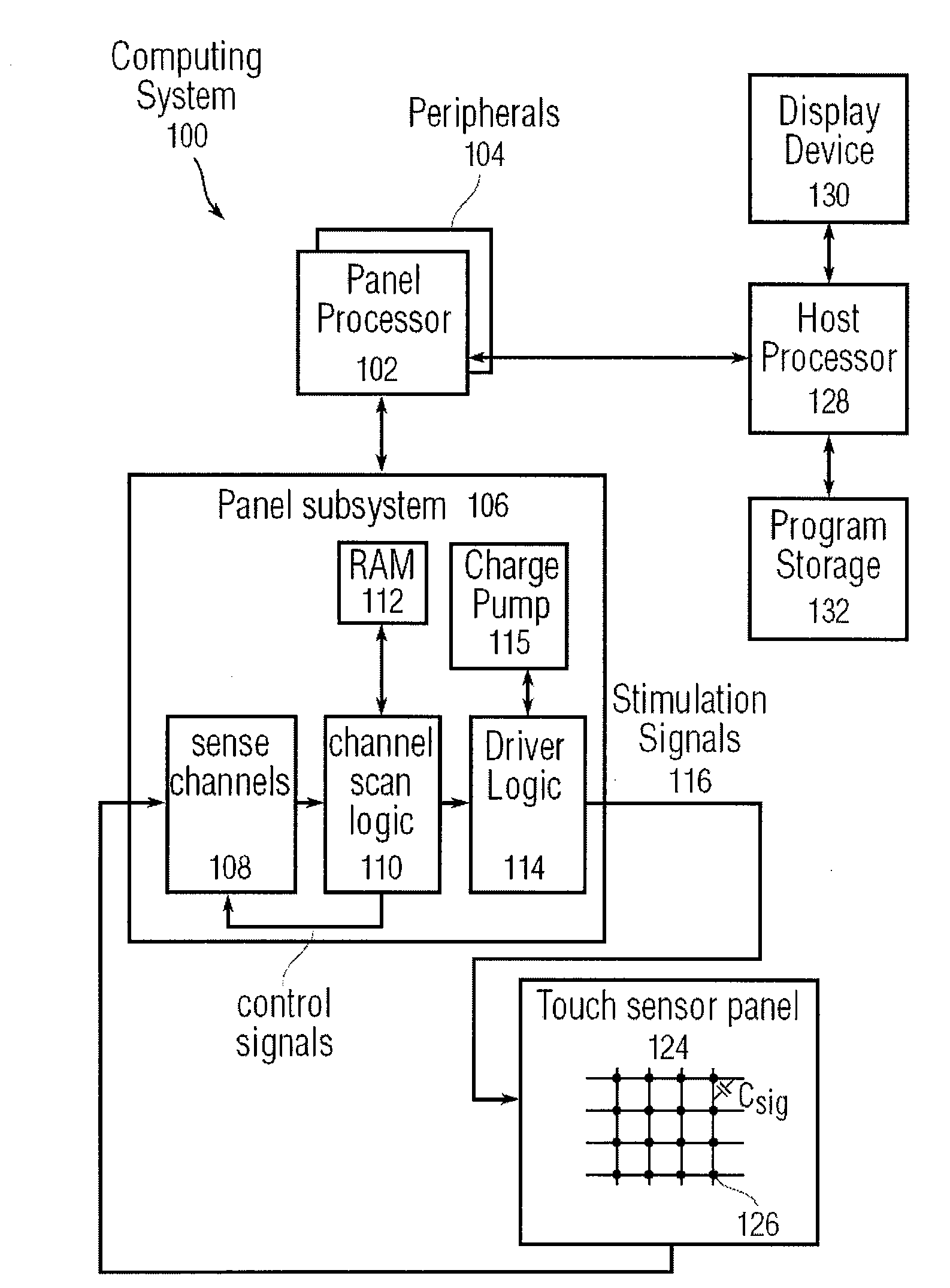
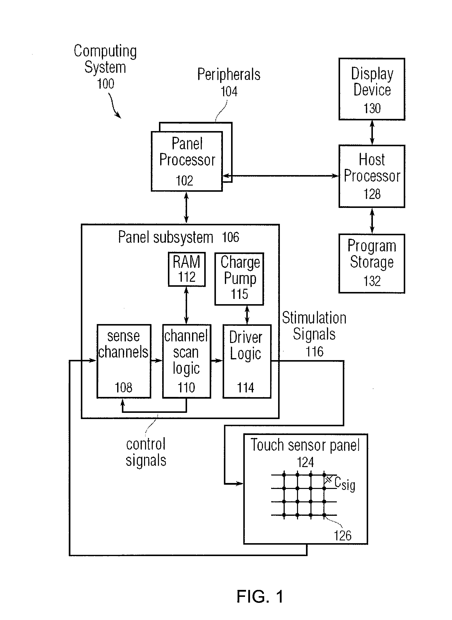
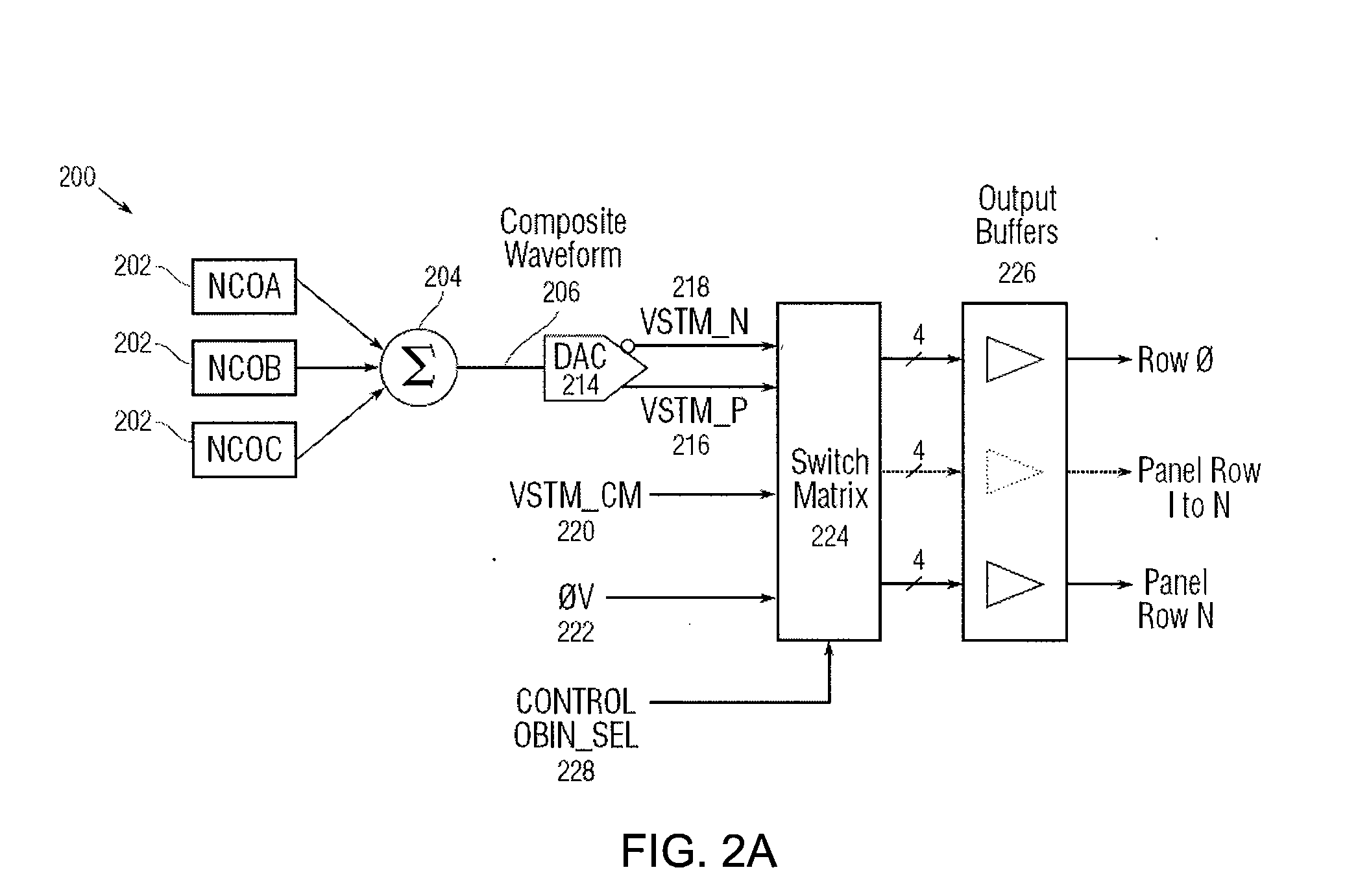
[0028]This relates to providing a cost and power effective architecture for detecting touch events on a touch sensor panel. In particular, drive logic, sense channels and channel scan logic can be provided on a single monolithic chip. Providing sensor panel circuitry on a single chip achieves hardware cost savings over multiple chip circuitry. The use of multiple stimulation frequencies and phases to sense touch events enables higher-power drive logic to operate with a reduced voltage on the same chip as lower-power sense channels. Further, channel scan logic can be provided to implement a sequence of scanning proce...


PUM


Abstract

A channel scan architecture for detecting touch events on a touch sensor panel is disclosed. The channel scan architecture can combine drive logic, sense channels and channel scan logic on a single monolithic chip. The channel scan logic can be configured to implement a sequence of scanning processes in a panel subsystem without intervention from a panel processor. The channel scan architecture can provide scan sequence control to enable the panel processor to control the sequence in which individual scans are implemented in the panel subsystem. Type of scans that can be implemented in the panel subsystem can include a spectral analysis scan, touch scan, phantom touch scan, ambient light level scan, proximity scan and temperature scan.

Description

FIELD OF THE INVENTION[0001]This relates to touch sensor panels that utilize multiple concurrent stimulation signals to detect and localize touch events, and more particularly, to a cost and power effective channel scan architecture capable of implementing a sequence of scans without intervention from a panel processor.BACKGROUND OF THE INVENTION[0002]Many types of input devices are presently available for performing operations in a computing system, such as buttons or keys, mice, trackballs, touch sensor panels, joysticks, touch screens and the like. Touch screens, in particular, are becoming increasingly popular because of their ease and versatility of operation as well as their declining price. Touch screens can include a touch sensor panel, which can be a clear panel with a touch-sensitive surface, and a display device that can be positioned behind the panel so that the touch-sensitive surface can substantially cover the viewable area of the display device. Touch screens can all...

Claims


Application Information

Patent Timeline
IPC IPC(8): G06F3/041
CPCG06F3/0416G06F3/04166G06F3/0418
Inventor WILSON, THOMAS JAMESKRAH, CHRISTOPH HORSTVU, MINH-DIEU THI
Owner APPLE INC
Learn More