Integrated Circuit Multilevel Inductor

Inactive Publication Date: 2010-03-04
APPLIED MICRO CIRCUITS CORPORATION
View PDF10 Cites 7 Cited by
  • Summary
  • Abstract
  • Description
  • Claims
  • Application Information

AI Technical Summary

Benefits of technology

[0007]The present invention IC multilayer inductor permits inductor cores to be eliminated from designs, producing more dies per wafer, and generally reducing fabrication and assembly costs. The IC multilayer can be used in signal tuning / peaking inductors and voltage-control oscillator tank applications, where the area size is limited and the quality factor requirement is not as strict. By constructing an inductor using metal evenly distributed between layers, “metal density” manufacturing design rules are met.

Problems solved by technology

The use of large inductors on PCBs results in higher costs, greater assembly complications, and a larger overall package size.
It is difficult to fabricate inductors integrally to a PCB.

Method used


Image

  • Integrated Circuit Multilevel Inductor
  • Integrated Circuit Multilevel Inductor
  • Integrated Circuit Multilevel Inductor

Examples


Embodiment Construction

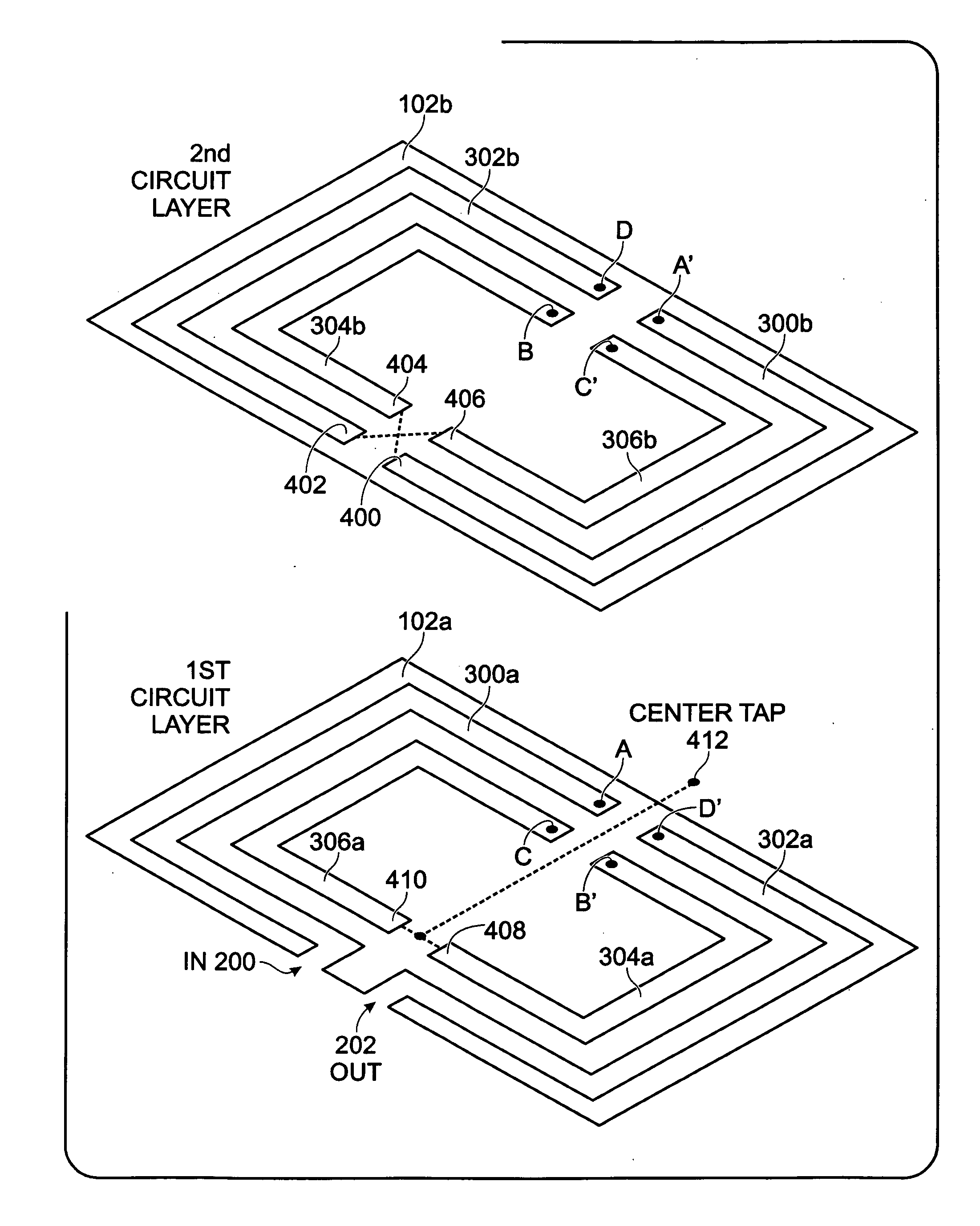
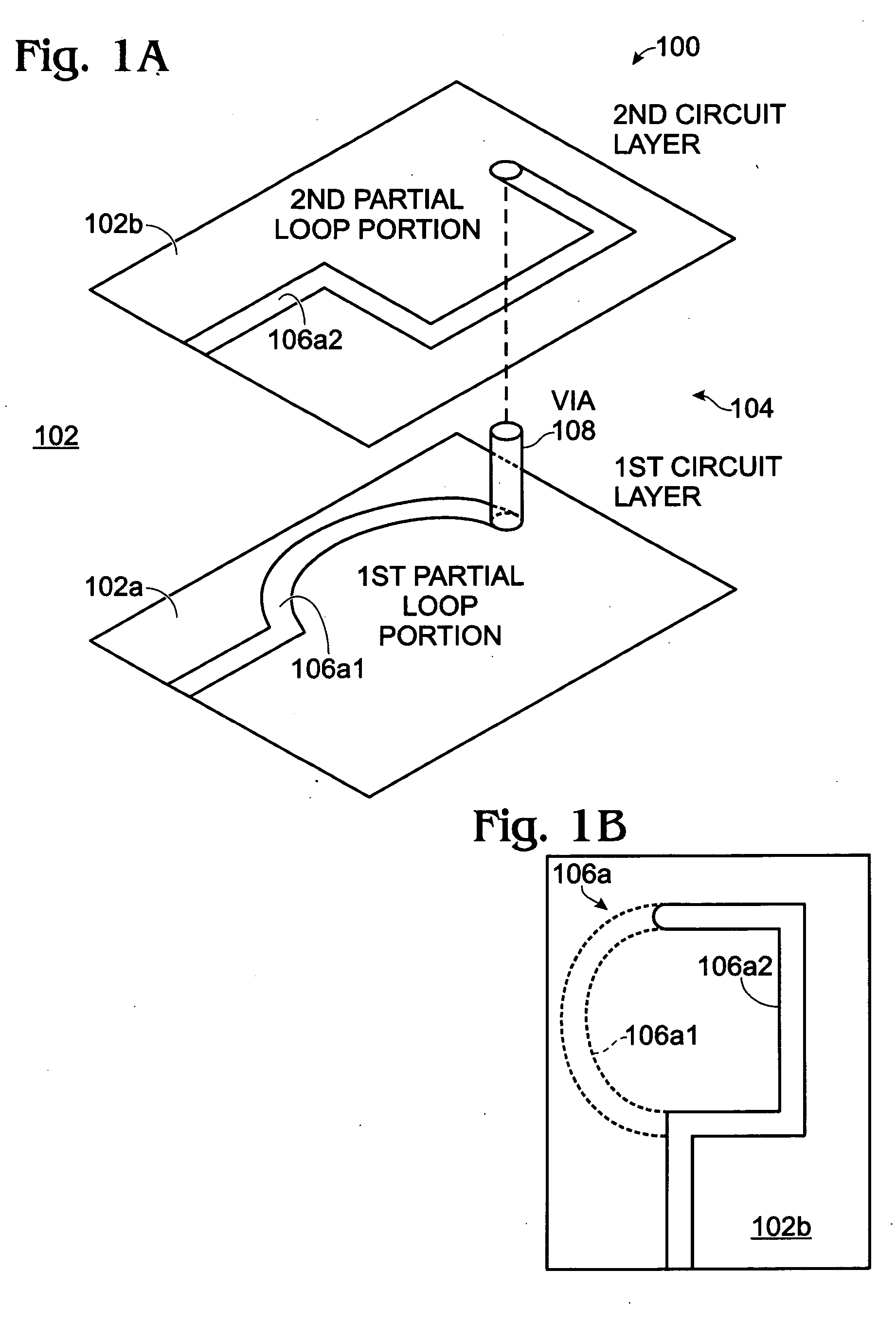
[0016]FIGS. 1A and 1B are perspective and plan views, respectively, depicting an integrated circuit (IC) multilevel inductor structure. The inductor structure 100 comprises an IC 102 including a plurality of circuit layers. First circuit layer 102a and second circuit layer 102b are shown. It should be understood that the IC typically includes other features on layers 102a and 102b, not shown, as well as additional circuit layers or interlevels (not shown). Typically, a dielectric material (not shown), such as silicon oxide, is interposed between circuit layers. An inductor 104 including a three-dimensional (3D) loop 106a is formed over a plurality of the circuit layers. More explicitly, the inductor 3D loop 106a includes a first partial loop portion 106a1 formed on the first circuit layer 102a, and second partial loop portion 106a2 formed on the second circuit layer 102b. A via 108 connects the first partial loop portion 106a1 and second partial loop portion 106a2.

[0017]As viewed fr...


PUM


Abstract

An integrated circuit (IC) multilevel inductor structure is provided. The IC multilayer inductor structure is made from an IC including a plurality of circuit layers, where the inductor is a three-dimensional (3D) loop formed over a plurality of the circuit layers. In a simple example, if the IC includes a first circuit layer and a second circuit layer, then the inductor 3D loop includes a first partial loop portion formed on the first circuit layer, a second partial loop portion formed on the second circuit layer, and a via connecting the first and second partial loop portions. More generally, the inductor typically includes a plurality of 3D loops. A first plurality of 3D loops is formed between the input and an nth circuit layer, and a second plurality of 3D loops is formed between the nth circuit layer and the output.

Description

BACKGROUND OF THE INVENTION[0001]1. Field of the Invention[0002]This invention generally relates to integrated circuit (IC) fabrication and, more particularly, to a multilayer inductor suitable for IC applications.[0003]2. Description of the Related Art[0004]Conventional digital systems fabricated on a single printed circuit board (PCB) or a collection of connected PCBs still often require analog circuitry. For example, analog circuits are often used in active buffers to boost a signal between communication nodes, or as an oscillator to create a reference signal. In both applications, inductors are used to peak or tune the signal to a desired frequency. The problem is that inductors tend to be large bulky components, and the electrical performance of bigger inductors (with higher quality (Q) factors and lower loss) is generally more desirable. The use of large inductors on PCBs results in higher costs, greater assembly complications, and a larger overall package size.[0005]It is dif...

Claims


Application Information

Patent Timeline
IPC IPC(8): H01F5/00
CPCH01F5/003H01F17/0013H01L23/5227H01L23/645H01L2924/0002H01L2924/00
Inventor FAN, SIQI
Owner APPLIED MICRO CIRCUITS CORPORATION
Why Eureka
Try Eureka