
Capacitive Touch Screen with Noise Suppression

a capacitive transducer and capacitive touch technology, applied in the field of capacitive touch screens or capacitive transducers 2dct sensors, can solve the problems of affecting capacitive measurements, affecting the accuracy of capacitive measurements, and requiring more electrodes, so as to reduce the susceptibility to coupling noise from a touch and improve linearity.

Active Publication Date: 2010-02-25
NEODRON LTD +1
View PDF24 Cites 179 Cited by
  • Summary
  • Abstract
  • Description
  • Claims
  • Application Information

AI Technical Summary

Benefits of technology

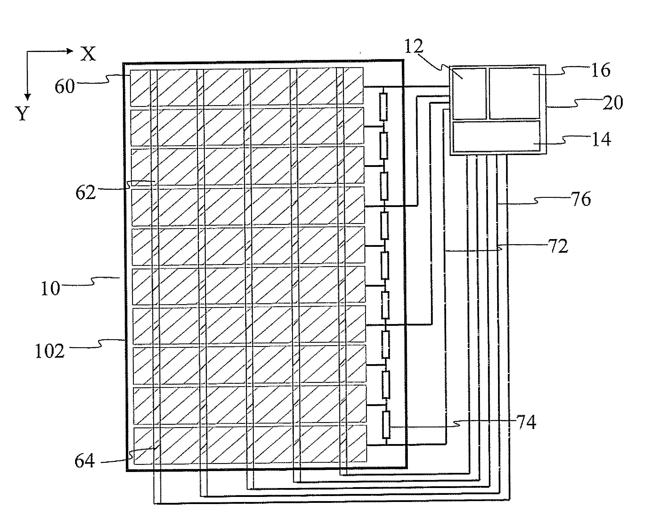
[0028]This approach has several important advantages. The touch sensor only requires the two layers of electrodes recited above to function, so that a third noise-suppressing layer as adopted in some prior art designs is superfluous. A two layer construction also leads to improved optical transmission, thinner overall depth and lower cost compared with designs with a greater numbers of layers. The area-filling design for the drive electrodes with small gaps allows for an almost invisible drive electrode pattern, for example when using ITO, and also isolates the sense lines from capacitive effects below the first layer, for example noise from an underlying LCD module or other noise source. The “flooding” of the first layer with conductive material also allows the second layer to be implemented with narrow sense electrodes, far narrower than the dimension of the sensing object. The second layer can also be made invisible either through in-filling of islands of electrode material between the sense electrodes to also “flood” the second layer, or alternatively simply by making the sense electrodes very thin or very sparse with line widths so small that they are invisible. This sparse approach using meshes is described further below. The reduced sense electrode area also reduces susceptibility to coupling noise from touches.
[0068]The Y-electrodes of the two-dimensional touch screen may further comprise a plurality of equally disposed cross-members running in the first direction. This can achieve uniform field patterns that are symmetrical in all regions of the touch screen leading to good linearity. These cross members effectively act to spread the electric field further beyond the primary Y-electrode to overlap the region which can gradate the electric field.

Problems solved by technology

ITO has desirable properties in optical terms, but can be substantially ohmic which can have a negative impact on capacitive measurements if the resistance and capacitance combination leads to time constants that prevent timely settling of the charge transfer process.
This region typically presents difficult challenges in this regard because of the non-uniformity of the electrode pattern (its ends) and the fact that interconnecting tracks tend to reside at the edges of the sensor.reducing the total number of electrodes used as each electrode requires some connection to the control chip and so more electrodes equates to a more complex chip and hence higher cost.
Linearity is one of the primary measures of quality of a touch screen because as the linearity degrades, it becomes harder to report an accurate touch location in some regions of the screen.
However, 2DCT sensors can be sensitive to external ground loading.
Furthermore, electrical noise generated from LCD screens can interfere with capacitance measurements when a pointing object approaches the screen.
However, the methods described above increase the size and thickness, and may decrease the resolution of a device incorporating a display screen with a 2DCT sensor when it is more fashionable and desirable to produce smaller devices.
Furthermore, additional steps are required during manufacture and as a result there is an increased cost due to further components being needed.
However, noise reduction techniques such as those described above require more complex measurement circuitry.
This makes the measurement circuitry more expensive and may increase the time taken to complete an acquisition cycle.

Method used


Image

  • Capacitive Touch Screen with Noise Suppression
  • Capacitive Touch Screen with Noise Suppression
  • Capacitive Touch Screen with Noise Suppression

Examples


Embodiment Construction

[0094]Described herein is a two-electrode layer construction for a capacitive touch screen or 2DCT sensor.

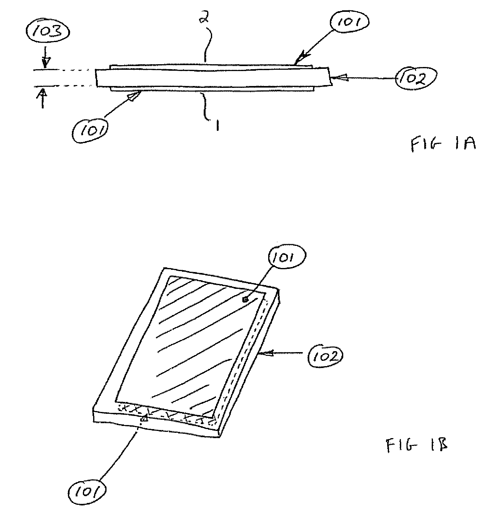
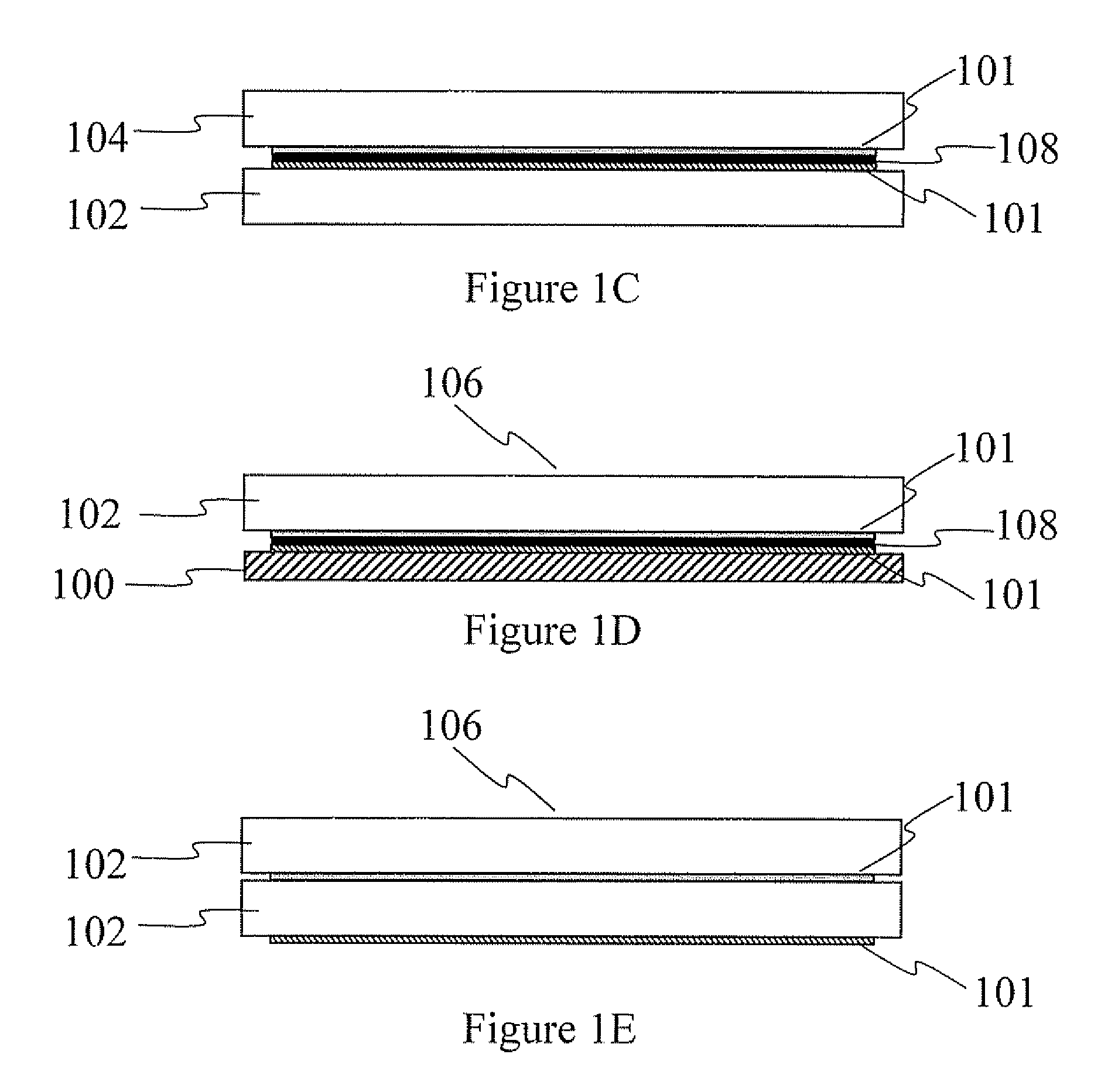
[0095]FIGS. 1A and 1B are schematic drawings in side view and perspective view of a two-electrode layer construction for a capacitive touch screen or 2DCT sensor. The layers 101 can generally be made of any conductive material and the layers can be arranged to oppose each other on two sides of any isolating substrate 102 such as glass, PET, FR4 etc. The thickness of the substrate 103 is non critical. Thinner substrates lead to higher capacitive coupling between the layers which must be mitigated in the control chip. Thicker substrates decrease the layer to layer coupling and are generally more favorable for this reason (because the measured change in capacitance is a larger fraction of the layer-to-layer capacitance so improving signal-to-noise ratio). Typical substrate thickness' range from 10's to 100's of μm. Furthermore it will appreciated that a dielectric or isolating laye...


PUM


Abstract

A capacitive touch sensor wherein the touch sensitive panel has drive electrodes arranged on the lower side of a substrate and sense electrodes arranged on the upper side. The drive electrodes are shaped and dimensioned to substantially entirely cover the touch sensitive area with individual drive electrodes being separated from each other by small gaps, the gaps being so small as to be practically invisible. The near blanket coverage by the drive electrodes also serves to screen out interference from noise sources below the drive electrode layer, such as drive signals for an underlying display, thereby suppressing noise pick-up by the sense electrodes that are positioned above the drive electrodes.

Description

BACKGROUND OF THE INVENTION[0001]The following describes a new invention in the field of capacitive touch screens or 2-dimensional capacitive transducing (2DCT) sensors. U.S. Pat. No. 6,452,514, U.S. Pat. No. 7,148,704 and U.S. Pat. No. 5,730,165 disclose a capacitive measurement technique which makes it possible to create touch responsive transparent or opaque sensing regions that can detect human touch through several millimeters of plastic or glass. Described herein is a new structure for a touch screen that allows significant enhancement in both operation and appearance of the sensor.[0002]U.S. Pat. No. 6,452,514 describes a capacitive measurement technique which is incorporated by reference herein, that uses a transmit-receive process to induce charge across the gap between an emitting electrode and a collecting electrode (the transmitter and the receiver respectively, also referred to as X and Y). The capacitive sensing described in U.S. Pat. No. 6,452,514 may be referred to a...

Claims


Application Information

Patent Timeline
IPC IPC(8): G06F3/044
CPCG01D5/2405G06F3/044G06F2203/04112G06F3/0416G01B7/003G01B2210/58H03K17/9622G06F3/041661G06F3/0446G06F3/0445G06F1/16G06F3/0412G06F2203/04111H05K1/0296
Inventor SLEEMAN, PETERBRUNET, SAMUELTREND, MATTHEWPHILIPP, HARALD
Owner NEODRON LTD
Learn More