Light-Emitting Device and Driving Method Thereof

a technology of light-emitting devices and driving methods, which is applied in the direction of semiconductor devices, instruments, electrical apparatus, etc., can solve the problems of increasing vds, flexibly setting the operation point of the el element closer to the linear region in order to reduce vds, and reducing luminance of an el element cannot be suppressed, so as to suppress the deterioration of the characteristics of the driving transistor, the effect of reducing the amount of current flowing

Active Publication Date: 2010-01-21
SEMICON ENERGY LAB CO LTD
View PDF15 Cites 9 Cited by
  • Summary
  • Abstract
  • Description
  • Claims
  • Application Information

AI Technical Summary

Benefits of technology

[0044]According to one mode of the present invention, in order to compensate the reduction in luminance due to the deterioration of the EL element, the potential difference between the electrodes of the EL element is detected in the light-emitting period of the EL element, charge corresponding to the potential difference between the electrodes is accumulated in the storage capacitor, the degree of deterioration of the EL element is calculated based on this charge, and the power source potential or the reference potential of the EL element is changed. After the charge corresponding to this potential difference is accumulated in the storage capacitor, the light emission of the EL element may be decayed; or alternatively, the potential difference between the electrodes of the EL element is detected in the period in which the EL element emits light, so that the luminance of the EL element is compensated. In this manner, reduction in luminance due to decrease in the amount of current which flows into the EL element can be prevented. Further, the operation point of the driving transistor which is operated in the saturation region can be shifted to be closer to the linear region, and the voltage which is applied to the driving transistor can be decreased to suppress the deterioration of the characteristics of the driving transistor.

Problems solved by technology

Consequently, reduction in luminance of an EL element cannot be suppressed when deterioration of the EL element is large.
Further, although it is preferable that Vds be lower in considering the reliability of each driving transistor and the operation point of the EL element be positioned in the saturation region as near as possible to the linear region, flexibly setting the operation point of the EL element closer to the linear region in order to decrease Vds is difficult because the current supply capabilities of the driving transistors are fixed.
That is, considering the deterioration of the EL element sufficiently, it is necessary that the operation point of the EL element is apart from the linear region as far as possible, which results in an increase in Vds, so that deterioration of the driving transistor is larger.

Method used


Image

  • Light-Emitting Device and Driving Method Thereof
  • Light-Emitting Device and Driving Method Thereof
  • Light-Emitting Device and Driving Method Thereof

Examples


embodiment 1

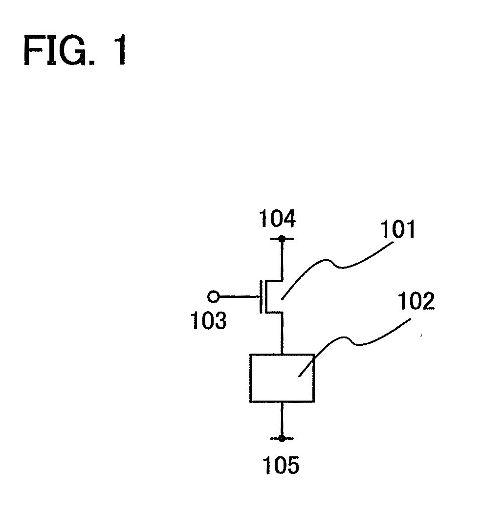
[0063]In FIG. 4A, a driving transistor 401, an EL element 402, and a first transistor (SW-1 Tr) 501 are shown. A gate of the driving transistor 401 is electrically connected to a first signal terminal 403. One of a source and a drain of the driving transistor 401 is electrically connected to a first power source terminal 404; and the other of the source and the drain thereof is electrically connected to one electrode (one of an anode and a cathode) of the EL element 402 and one of a source and a drain of the SW-1 Tr 501. A gate of the SW-1 Tr 501 is electrically connected to a second signal terminal 406; and the other of the source and the drain thereof is electrically connected to a signal detector circuit. The other electrode (the other of the anode and the cathode) of the EL element 402 is electrically connected to a second power source terminal 405.

[0064]The driving transistor 401 controls the amount of current which flows into the EL element 402 to determine the luminance of th...

embodiment 2

[0079]In the circuit in FIG. 4B, the gate of the SW-2 Tr 502 is electrically connected to the third signal terminal 407, and the other of the source and the drain of the SW-1 Tr 501 and one electrode of the Cs 503 are electrically connected to one of the source and the drain of the SW-2 Tr 502. The present invention is, however, not limited to this circuit. Without provision of the third signal terminal 407, the other of the source and the drain of the SW-1 Tr 501 and one electrode of the Cs 503 may be electrically connected to the gate of the SW-2 Tr 502, so that a signal corresponding to the potential difference of the electrodes of the EL element is conducted to the signal detector circuit (FIG. 7A).

[0080]A circuit shown in FIG. 7A includes a driving transistor 401, an EL element 402, a SW-i Tr 501, a SW-2 Tr 502, and a Cs 503. A gate of the driving transistor 401 is electrically connected to a first signal terminal 403. One of a source and a drain of the driving transistor 401 i...

embodiment 3

[0094]In this embodiment, the case where the present invention is applied to an active matrix display device in which a plurality of pixels is provided and an EL element is provided for each pixel will be described.

[0095]A circuit shown in FIG. 9 includes a driving transistor 601, an EL element 602, a SW-1 Tr 604, a SW-2 Tr 606, a first storage capacitor Cs 605, a fourth transistor (SW-4 Tr) 607, a second storage capacitor Cs 608, a first scanning line 610, a second scanning line 612, a signal line 609, and a power source line 611. A potential on the high-potential side of a power source (a power source potential, Vdd) is applied to the power source line 611; and a potential on the low-potential side of the power source (a reference potential) is applied to a power source terminal 603, in which the potential corresponds to the reference potential (Vcom) of the EL element 602.

[0096]A gate of the SW-4 Tr 607 is electrically connected to the first scanning line 610; one of a source and...


PUM


Abstract

Charge corresponding to a potential difference between electrodes of an electroluminescence element is accumulated in a period in which the electroluminescence element emits light; the potential difference is detected without decrease in the luminance at the time of light emission of the electroluminescence element; and a reference potential of one electrode of the electroluminescence element is changed based on the detected potential difference, so that reduction in luminance of the electroluminescence element due to deterioration of the electroluminescence element is compensated.

Description

BACKGROUND OF THE INVENTION[0001]1. Field of the Invention[0002]The present invention relates to a light-emitting device for compensating reduction in luminance of the light-emitting device.[0003]2. Description of the Related Art[0004]In recent years, wide-viewing-angle, high-moving-image-characteristics light-emitting devices using electroluminescence elements (EL elements) have been developed. The EL elements, which are self-emission elements that themselves emit light, have a problem in that the luminance is likely to decrease over time. When EL elements deteriorates, resistance thereof generally increases. Therefore, under a condition in which a certain voltage is applied to an EL element, the amount of current which flows into the EL element decreases as the EL element deteriorates, which cause reduction in the luminance.[0005]In FIG. 1, a driving transistor 101 and an EL element 102 which is electrically connected to the driving transistor101 are shown. A gate of the driving t...

Claims


Application Information

Patent Timeline
Patent Type & Authority Applications(United States)
IPC IPC(8): G09G3/30
CPCG09G3/3233G09G2300/0439H01L27/1251G09G2320/043G09G2320/045G09G2300/0819H10K59/12
Inventor HONDA, TATSUYA
Owner SEMICON ENERGY LAB CO LTD
Why Eureka
Try Eureka