
Development device

Inactive Publication Date: 2009-11-26
RICOH KK
View PDF32 Cites 16 Cited by
  • Summary
  • Abstract
  • Description
  • Claims
  • Application Information

AI Technical Summary

Benefits of technology

[0076]Thereafter, the coated metal substrate undergoes photolithographic processes to obtain a pattern of multiple electrodes thereon, followed by application of polyimide to obtain a protective layer over the patterned surface. In case the protective layer has an uneven surface due to gaps between the electrodes lying on the metal substrate, it is desirable to planarize the substrate surface by applying a polyimide or polyurethane material of a viscosity ranging from approximately 50 to approximately 10,000 centipoise (cP), preferably, from approximately 100 to approximately 300 cP with a spin coater, and leaving the substrate to stand until the coated surface becomes smooth owing to its surface tension.
[0016]In one exemplary embodiment, the novel development device includes an open-ended housing, a rotatable roller, an array of multiple electrodes, a voltage source, a sealing member, and a secondary electrode. The open-ended housing accommodates toner for application to the photoconductive surface through an end opening thereof. The rotatable roller has an outer circumferential surface thereof partially accommodated within the housing and partially facing the photoconductive surface through the end opening to deliver the toner from within the housing to a development zone defined between the roller surface and the photoconductive surface. The array of multiple electrodes are aligned parallel with each other on and extending longitudinally along the roller surface. The voltage source applies a periodic pulse voltage to at least a subset of the electrodes to generate an oscillating primary electric field under which the toner moves back and forth between neighboring primary electrodes and consequently jumps across the development zone to adhere to the electrostatic latent image. The sealing member seals clearance between the roller surface and an edge of the end opening. The voltage source energizes at least one of the electrodes closest to the sealing member with a direct current voltage of a polarity opposite to that of the toner to counteract an electrostatic force of the electric field repelling the toner from the roller surface.
[0051]Further, application of the antiphase voltages VA and VB to the electrodes 3a and 3b develops a periodically oscillating electric field on the circumferential surface of the developer roller 3. Upon loading onto the developer roller 3, toner particles periodically hop or move back and forth in parabolic orbits between neighboring electrodes 3a and 3b along electric field lines of the oscillating electric field to form a “flare” or aerosol cloud of periodically hopping toner particles around the roller surface.
[0016]In one exemplary embodiment, the novel development device includes an open-ended housing, a rotatable roller, an array of multiple electrodes, a voltage source, a sealing member, and a secondary electrode. The open-ended housing accommodates toner for application to the photoconductive surface through an end opening thereof. The rotatable roller has an outer circumferential surface thereof partially accommodated within the housing and partially facing the photoconductive surface through the end opening to deliver the toner from within the housing to a development zone defined between the roller surface and the photoconductive surface. The array of multiple electrodes are aligned parallel with each other on and extending longitudinally along the roller surface. The voltage source applies a periodic pulse voltage to at least a subset of the electrodes to generate an oscillating primary electric field under which the toner moves back and forth between neighboring primary electrodes and consequently jumps across the development zone to adhere to the electrostatic latent image. The sealing member seals clearance between the roller surface and an edge of the end opening. The voltage source energizes at least one of the electrodes closest to the sealing member with a direct current voltage of a polarity opposite to that of the toner to counteract an electrostatic force of the electric field repelling the toner from the roller surface.

Problems solved by technology

One common problem with a development device in which the developer roller is accommodated in an open-ended housing is leakage of toner from the housing opening.
That is, toner particles, stirred up within the developer chamber, leak through any clearance between the surface of the developer roller and edges of the housing opening.
Such leaking toner results in contamination of areas adjacent to the development device as well as smudges on recording media (e.g., sheets of paper, etc.) passing through the contaminated surfaces during image formation.
Unfortunately, the conventional sealing technique is not compatible with a hopping development device described above.
Naturally, such migration of toner results in reduced efficiency of toner delivery to or from the development zone, causing various adverse effects on the performance of the image forming apparatus employing the hopping development device.
This results in development deficiencies due to insufficient supply of toner in the development zone, even when the developer roller is loaded with proper amounts of toner inside the developer chamber.
This results in toner particles accumulating on the sealing blade and eventually spreading out to contaminate areas adjacent to the development device.
However, such a configuration is impractical because the alleviation is ineffective when the edge-to-surface gap is greater than the height to which toner particles jump from the roller surface.

Method used


Image

  • Development device
  • Development device
  • Development device

Examples


Embodiment Construction

[0034]In describing exemplary embodiments illustrated in the drawings, specific terminology is employed for the sake of clarity. However, the disclosure of this patent specification is not intended to be limited to the specific terminology so selected, and it is to be understood that each specific element includes all technical equivalents that operate in a similar manner and achieve a similar result.

[0035]Referring now to the drawings, wherein like reference numerals designate identical or corresponding parts throughout the several views thereof, exemplary embodiments of the present patent application are described.

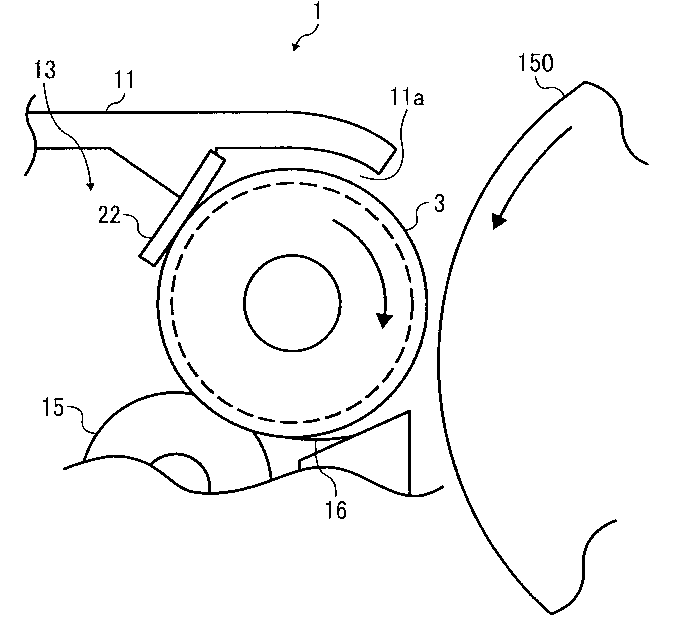
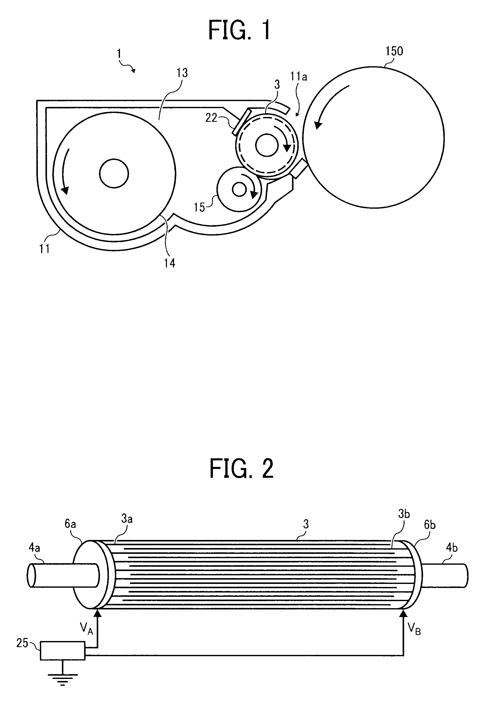
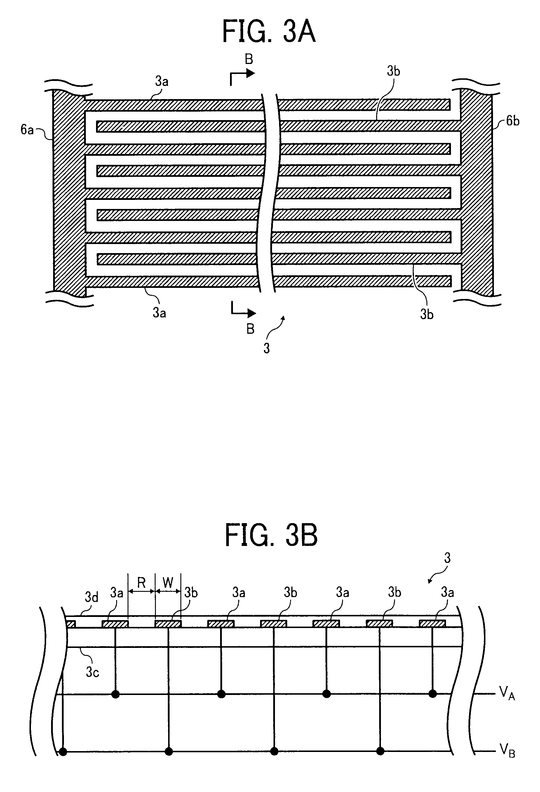
[0036]FIG. 1 schematically illustrates a general configuration of a development device 1 according to this patent specification.

[0037]As shown in FIG. 1, the development device 1 includes an open-ended housing 11 defining a developer chamber 13 that accommodates developer and / or toner particles for application to a photoconductive drum 150 through an end opening 11a. The...


PUM


Abstract

A development device includes an open-ended housing, a rotatable roller, an array of multiple primary electrodes, a voltage source, a sealing member, and a secondary electrode. The housing accommodates toner for application to the photoconductive surface through an end opening thereof. The roller has an outer circumferential surface to deliver the toner from within the housing to a development zone. The array of multiple primary electrodes are aligned with each other on the roller surface. The voltage source applies a periodic pulse voltage to at least a subset of the primary electrodes to generate an oscillating primary electric field. The sealing member seals clearance between the roller surface and an edge of the end opening downstream from the development zone. The secondary electrode generates a secondary electric field to force the toner from the sealing member toward the roller surface to prevent premature removal of the toner.

Description

CROSS-REFERENCE TO RELATED APPLICATIONS[0001]The present patent application claims priority pursuant to 35 U.S.C. §119 from Japanese Patent Application No. 2008-133426 filed on May 21, 2008, the contents of which are hereby incorporated by reference herein in their entirety.BACKGROUND OF THE INVENTION[0002]1. Field of the Invention[0003]The present invention relates to a development device, and more particularly, to a development device including a developer roller that generates an oscillating electric field under which charged toner particles jump across a development gap to develop an electrostatic latent image recorded on a photoconductive surface.[0004]2. Discussion of the Background[0005]In electrophotographic image formation, development devices are used to develop an electrostatic latent image recorded on a photoconductive surface with charged toner particles. Generally, an electrophotographic development device includes an open-ended developer housing defining a developer c...

Claims


Application Information

Patent Timeline
IPC IPC(8): G03G15/08
CPCG03G15/0817G03G2215/0653G03G15/0818
Inventor ISHII, YASUYUKIKOSUGI, HIDEKITAKAHASHI, TOMOKONAKAGAWA, YOSHINORIYAMADA, MASAAKIKADOTA, ICHIRO
Owner RICOH KK
Learn More