
Method of manufacturing silicon nano-structure

a technology of silicon nano-structure and manufacturing method, which is applied in the direction of nanoinformatics, crystal growth process, polycrystalline material growth, etc., can solve the problems of high melting point, low growth efficiency, and increased cos

Active Publication Date: 2009-10-08
TSINGHUA UNIV +1
View PDF8 Cites 17 Cited by
  • Summary
  • Abstract
  • Description
  • Claims
  • Application Information

AI Technical Summary

Benefits of technology

[0002]The present invention relates to methods for making nano materials and, particularly, to a method for making a silicon nano-structure.

Problems solved by technology

However, there are some drawbacks to using this method.
Firstly, the step of forming a metal catalyst layer on the wafer is usually preformed in vacuum and requires a depositing device, thus increasing costs.
Secondly, the metal catalyst is gold, copper or iron, which have high melting points and low growing efficiency.

Method used


Image

  • Method of manufacturing silicon nano-structure
  • Method of manufacturing silicon nano-structure
  • Method of manufacturing silicon nano-structure

Examples


Embodiment Construction

[0014]References will now be made to the drawings to describe, in detail, various embodiments of the present method for making a silicon nano-structure.

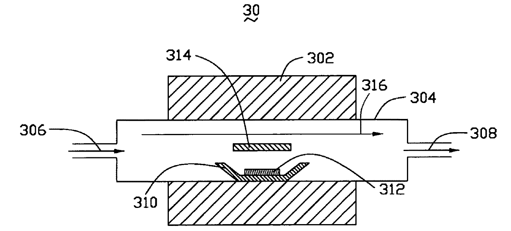
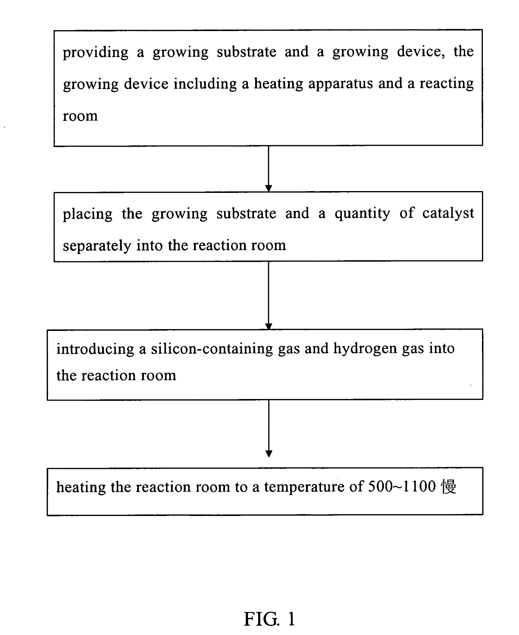
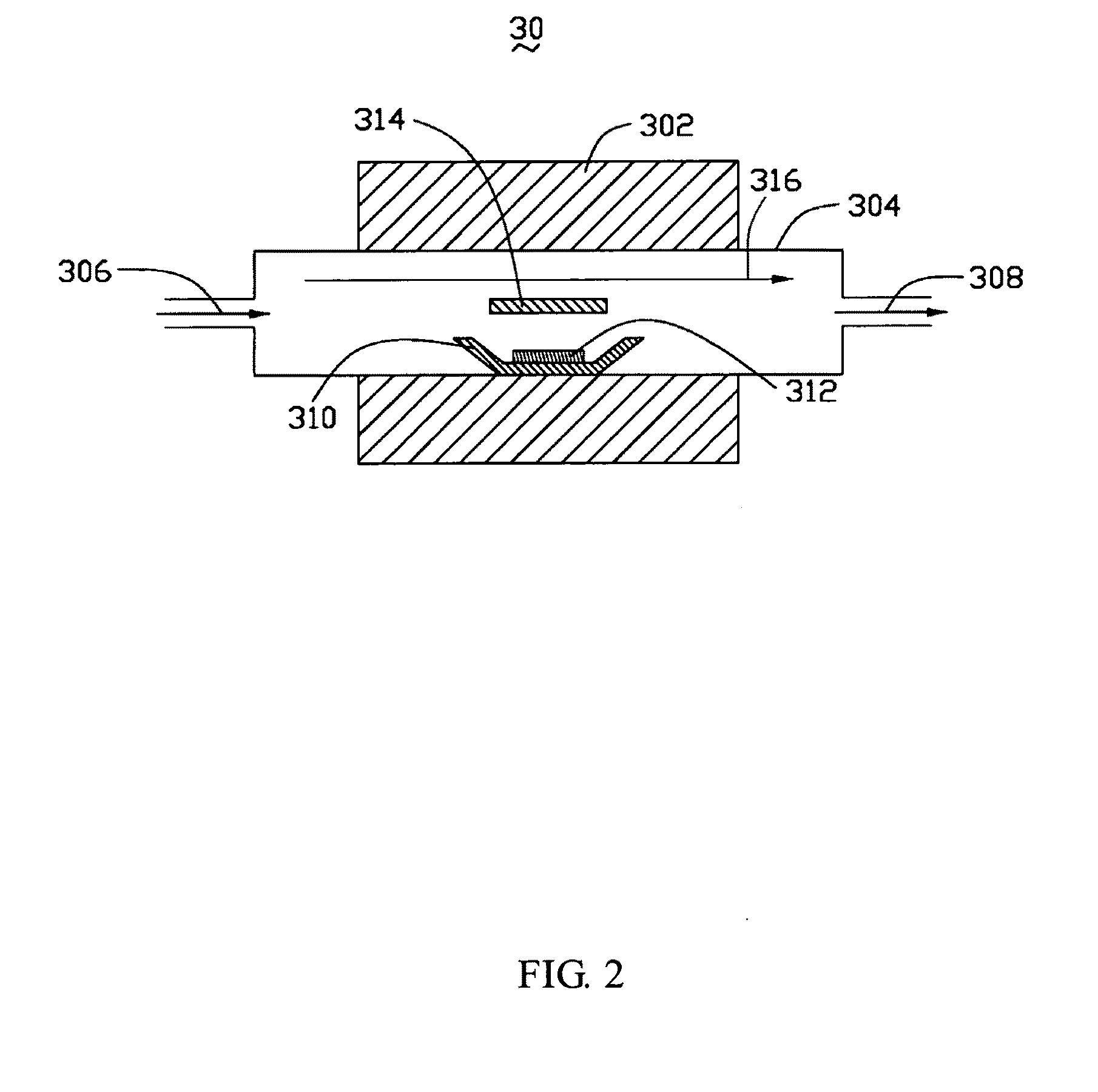
[0015]Referring to FIGS. 1 and 2, a method for making a silicon nano-structure includes the following steps: (a) providing a growing substrate 314 and a growing device 30, the growing device 30 including a heating apparatus 302 and a reacting room 304; (b) placing the growing substrate 314 and a quantity of catalyst 312 separately into the reacting room 304; (c) introducing a silicon-containing gas and hydrogen gas into the reacting room 304; and (d) heating the reacting room to a temperature of 500˜1100° C.

[0016]In step (a), the reacting room 304 can be a quartz tube with a gas inlet 306 at one end and a gas outlet 308 at an opposite end. The quartz tube is movably located in the heating apparatus 302. The length of the quartz tube is more than the length of the heating apparatus 302 so that part of the tube can be used as a handle ...


PUM


Abstract

A method for making silicon nano-structure, the method includes the following steps. Firstly, providing a growing substrate and a growing device, the growing device comprising a heating apparatus and a reacting room. Secondly, placing the growing substrate and a quantity of catalyst separately into the reacting room. Thirdly, introducing a silicon-containing gas and hydrogen gas into the reacting room. Lastly, heating the reacting room to a temperature of 500˜1100° C.

Description

BACKGROUND[0001]1. Field of the Invention[0002]The present invention relates to methods for making nano materials and, particularly, to a method for making a silicon nano-structure.[0003]2. Discussion of Related Art[0004]Silicon is one of the most favored materials in the semiconductor industry, and it has been used in the IC industry for many years. Silicon nano materials have been applied in such things as field emission electronic devices, solar batteries and diluted magnetic semiconductor devices, due to their outstanding mechanical and electrical properties. Therefore, achieving various silicon nano materials is desirable.[0005]A conventional method for making a silicon nano material includes the following steps: providing a silicon wafer; forming a metal catalyst layer on a surface of the wafer; putting the wafer with catalyst layer into a quartz tube; introducing a silicon-containing gas and hydrogen gas into the quartz tube; and heating the quartz tube to a temperature of 50...

Claims


Application Information

Patent Timeline
Patent Type & Authority Applications(United States)
IPC IPC(8): H01L21/20
CPCB82Y10/00B82Y30/00C30B29/06Y10S977/855Y10S438/903Y10S977/857C30B29/60
Inventor SUN, HAI-LINJIANG, KAI-LILI, QUN-QINGFAN, SHOU-SHAN
Owner TSINGHUA UNIV
Learn More