
Method for controlling spatial temperature distribution across a semiconductor wafer

a technology of spatial temperature distribution and semiconductor wafer, which is applied in the direction of semiconductor/solid-state device testing/measurement, electrical equipment, electric discharge tubes, etc., can solve the problems of significant and progressive pressure loss across the sealing land, the edge of the wafer 104/b> may be inadequately cooled, and the difficulty of ensuring uniformity of each batch of ics from larger and larger wafers

Active Publication Date: 2009-08-27
LAM RES CORP
View PDF47 Cites 42 Cited by
  • Summary
  • Abstract
  • Description
  • Claims
  • Application Information

AI Technical Summary

Problems solved by technology

Local wafer temperature and rate of reaction at each microscopic point on the wafer are related to an extent that harmful unevenness in etching of material over a face of the wafer can easily result if the temperature of the wafer across its area varies too much.
Furthermore, with each increase in the size of wafer diameter, the problem of ensuring uniformity of each batch of ICs from larger and larger wafers becomes more difficult.
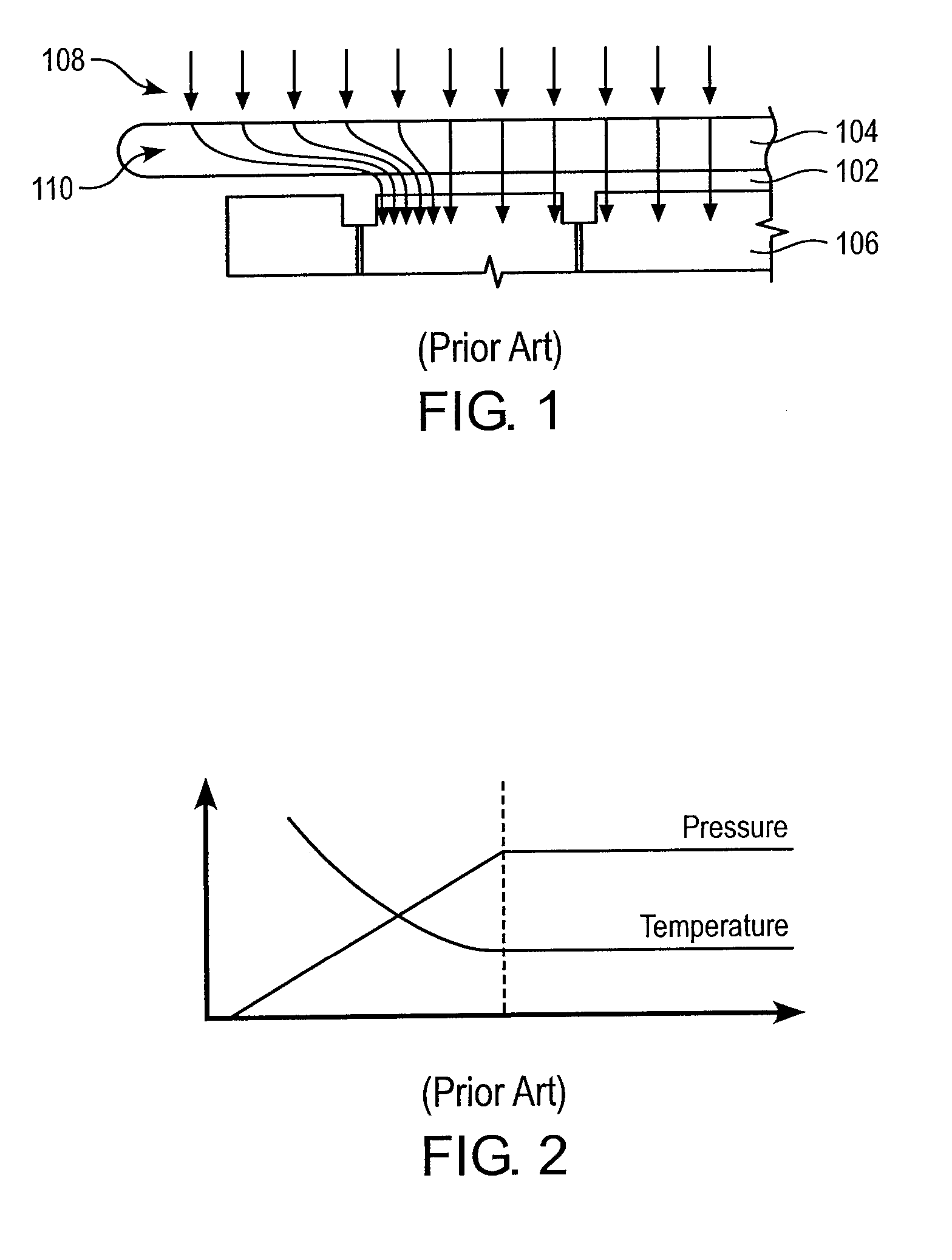
Inevitably, without any elastomer seal there is significant and progressive pressure loss across the sealing land, such that the edge of the wafer 104 may be inadequately cooled.
However the local contact area can only be adjusted by re-machining the chuck.
This is relatively effective at high power flux but will only give small temperature differentials at lower power flux.
However, other processes may run at low power, for instance poly gate processes, may have a flux of only 0.2 W per cm2.
Unless the average conduction is made extremely low, which is very difficult to control and tends to result in inadequate overall cooling, then there will be only a very small differential of typically less than 5° C.

Method used


Image

  • Method for controlling spatial temperature distribution across a semiconductor wafer
  • Method for controlling spatial temperature distribution across a semiconductor wafer
  • Method for controlling spatial temperature distribution across a semiconductor wafer

Examples


Embodiment Construction

[0020]Embodiments of the present invention are described herein in the context of a workpiece support. Those of ordinary skill in the art will realize that the following detailed description of the present invention is illustrative only and is not intended to be in any way limiting. Other embodiments of the present invention will readily suggest themselves to such skilled persons having the benefit of this disclosure. Reference will now be made in detail to implementations of the present invention as illustrated in the accompanying drawings. The same reference indicators will be used throughout the drawings and the following detailed description to refer to the same or like parts.

[0021]In the interest of clarity, not all of the routine features of the implementations described herein are shown and described. It will, of course, be appreciated that in the development of any such actual implementation, numerous implementation-specific decisions must be made in order to achieve the dev...


PUM

PropertyMeasurementUnit
temperatureaaaaaaaaaa
pressureaaaaaaaaaa

Abstract

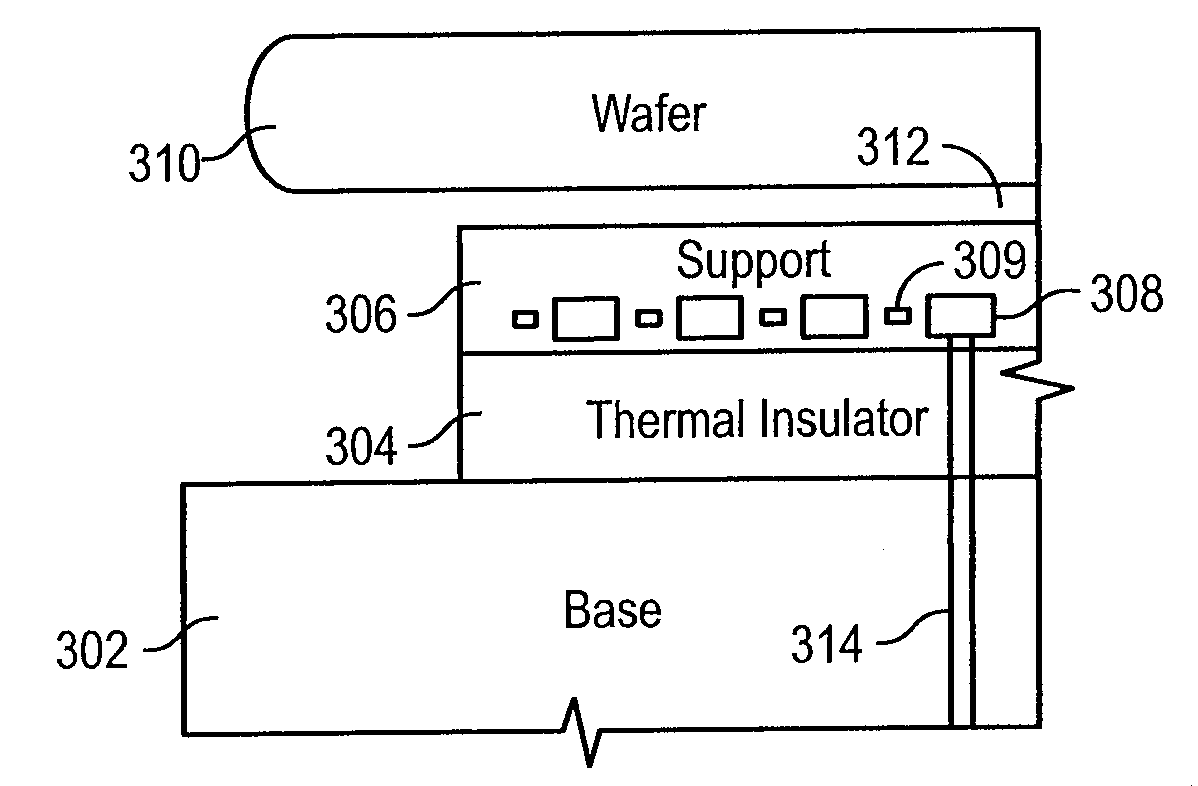
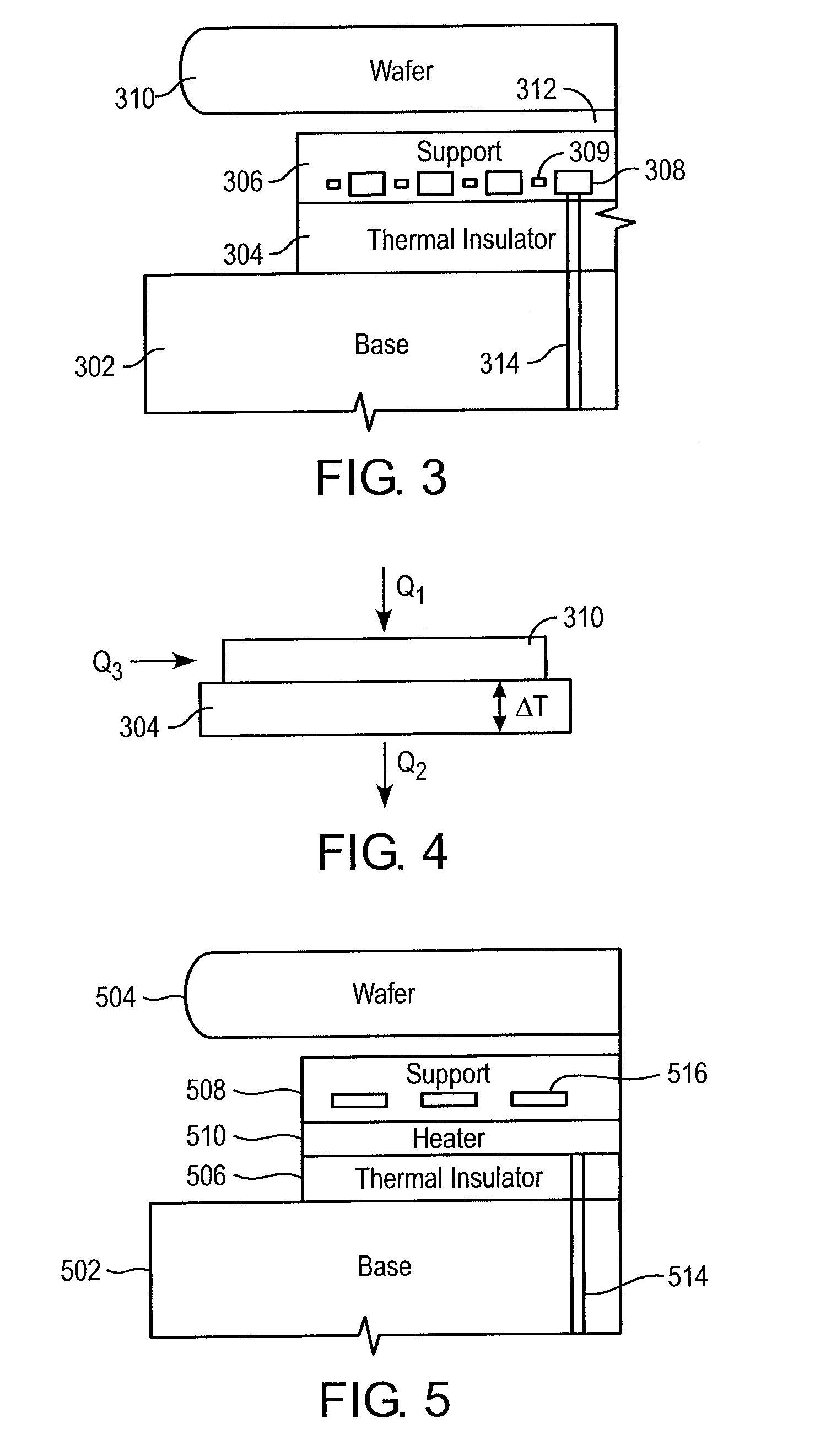
A chuck for a plasma processor comprises a temperature-controlled base, a thermal insulator, a flat support, and a heater. The temperature-controlled base is controlled in operation a temperature below the desired temperature of a workpiece. The thermal insulator is disposed over at least a portion of the temperature-controlled base. The flat support holds a workpiece and is disposed over the thermal insulator. A heater is embedded within the flat support and / or mounted to an underside of the flat support. The heater includes a plurality of heating elements that heat a plurality of corresponding heating zones. The power supplied and / or temperature of each heating element is controlled independently. The heater and flat support have a combined temperature rate change of at least 1° C. per second.

Description

CROSS-REFERENCES[0001]This is a continuation-in-part of U.S. patent application Ser. No. 10 / 062,395, filed Feb. 1, 2002, which is, in turn, a continuation-in-part of U.S. patent application Ser. No. 09 / 846,432, filed Apr. 30, 2001, in the name of inventors Neil Benjamin and Robert Steger, entitled “Method and Apparatus for controlling the spatial temperature distribution across the surface of a workpiece support”, commonly assigned herewith.FIELD OF THE INVENTION[0002]The present invention relates to substrate support. More particularly, the present invention relates to a method and apparatus for achieving uniform temperature distribution within a substrate during plasma processing.BACKGROUND OF THE INVENTION[0003]A typical plasma etching apparatus comprises a reactor in which there is a chamber through which reactive gas or gases flow. Within the chamber, the gases are ionized into a plasma, typically by radio frequency energy. The highly reactive ions of the plasma gas are able to...

Claims


Application Information

Patent Timeline
Patent Type & Authority Applications(United States)
IPC IPC(8): H01L21/465H01L21/66C23F4/00H01L21/00H01L21/02H01L21/3065H01L21/683
CPCH01J2237/2001H01L21/67069H01L21/68714H01L21/67248H01L21/6833H01L21/67103H01J37/32724H01L21/683H01J2237/334
Inventor BENJAMIN, NEILSTEGER, ROBERT
Owner LAM RES CORP
Learn More