
Thermal infrared detecting device

a technology of infrared detection and infrared light, which is applied in the field of thermal infrared detection devices, can solve the problems of insufficient exertion, inability to solve the negative feedback effect, and high sensitivity, and achieve the effect of eliminating the negative feedback effect caused by the interconnection resistan

Active Publication Date: 2009-08-06
MITSUBISHI ELECTRIC CORP
View PDF9 Cites 13 Cited by
  • Summary
  • Abstract
  • Description
  • Claims
  • Application Information

AI Technical Summary

Benefits of technology

[0015]The present invention is directed to solve the foregoing problem, and has an object to provide a high-sensitivity thermal infrared detecting device capable of suppressing the negative feedback effect caused by the interconnection resistance.
[0016]In order to solve the above problem, in a thermal infrared detecting device according to the present invention, the bias voltage applied between both ends of the diode is controlled at a constant value irrespective of the current flowing through the diode which has a heat-insulated structure and an infrared absorption section. Therefore, the voltage across the diode is always kept constant even if the diode temperature is changed and the diode current is changed. This configuration allows the negative feedback effect caused by the interconnection resistance to be reduced. More specifically, the thermal infrared detecting device according to the present invention has the following configuration.
[0018]According to the present invention, the voltage across the diode is always kept at a value obtained by subtracting the predetermined bias voltage from the power supply voltage, even if the diode temperature is changed and therefore the diode current varies. Thus, the negative feedback effect caused by the interconnection resistance can be eliminated to realize the high-sensitivity thermal infrared detecting device.

Problems solved by technology

The following problem may be generated when a predetermined bias is applied to the diode under the high electric resistance of the interconnection.
The negative feedback effect causes a problem in that a characteristic of high sensitivity as the feature of the constant-voltage drive scheme cannot sufficiently be exerted.
However, the method cannot solve the negative feedback effect caused by the resistances of the signal line and selection line to the column transistors as the voltage converting means and the interconnection resistance in the pixel.
However, in the method, it is clear that the negative feedback effect caused by the interconnection resistance generated in the incidence of the infrared ray cannot be eliminated.
Therefore, similarly to JP-A-2000-019015, JP-A-2001-044400 does not solve the problem of the negative feedback effect caused by the interconnection resistance generated in the incidence of the infrared ray.
JP-A-2001-264176 describes the negative feedback effect caused by the resistance, and points out that the negative feedback effect becomes troublesome when a resistor connected for reading the current and raising the output is increased.

Method used


Image

  • Thermal infrared detecting device
  • Thermal infrared detecting device
  • Thermal infrared detecting device

Examples


first embodiment

1. Entire Configuration of Thermal Infrared Detecting Device

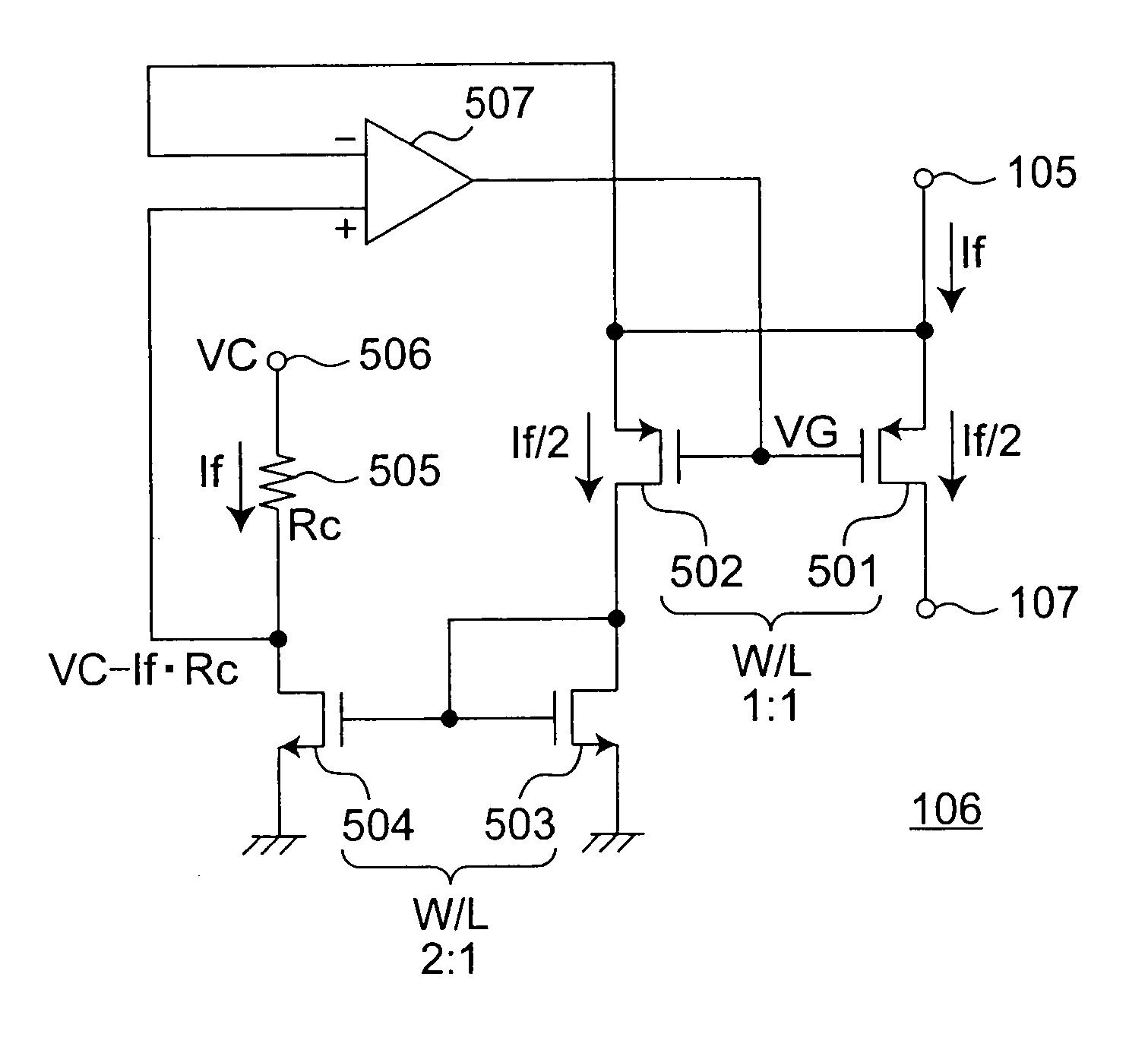
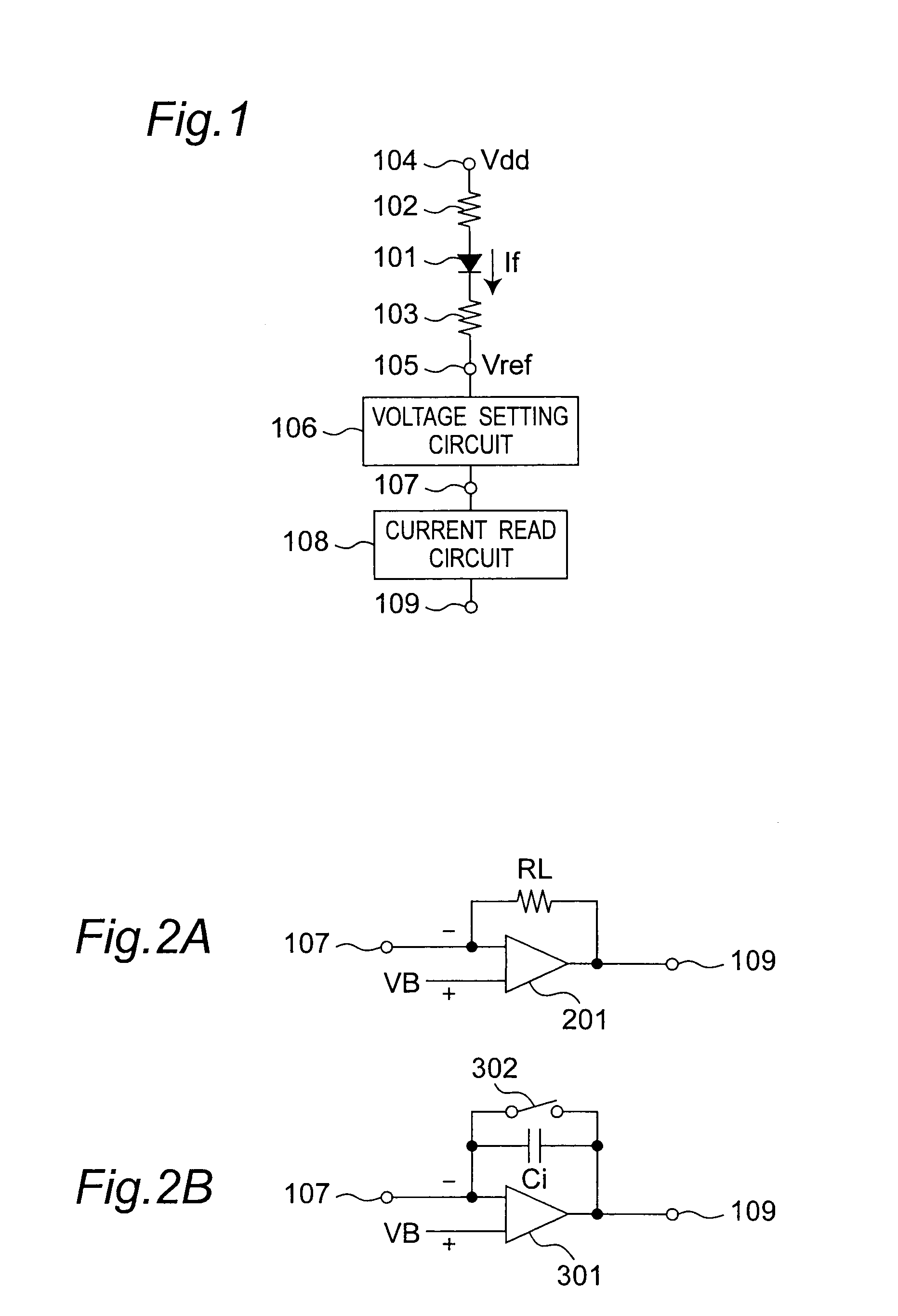
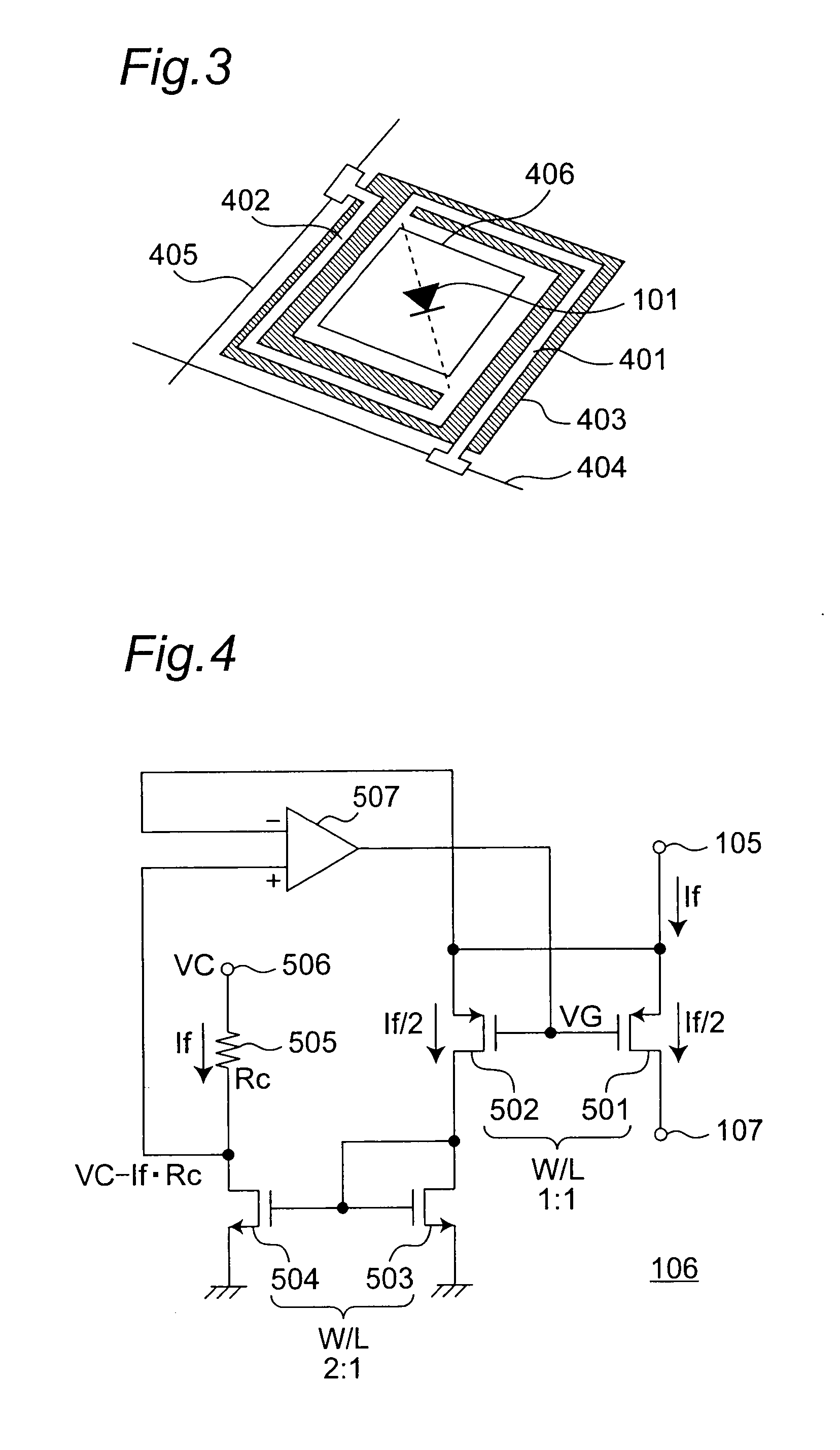
[0055]FIG. 1 shows a configuration of a thermal infrared detecting device according to a first embodiment of the present invention. For convenience of explanation, FIG. 1 shows a configuration for a single pixel (including a single diode for detecting infrared ray). The thermal infrared detecting device includes an infrared detecting diode 101. An anode of the infrared detecting diode 101 is connected to a power supply terminal 104 through a resistor 102, and a cathode is connected to a voltage setting circuit 106 through a resistor 103 and a terminal 105. A current If flowing through the diode 101 enters a current read circuit 108 through the voltage setting circuit 106 and a terminal 107, and is detected through a terminal 109. Although the terminals 105 and 107 are expressed as terminal for the sake of convenience, the terminals 105 and 107 may be formed in other form as long as those are electrically connected.

[0056]The...

second embodiment

[0067]FIG. 5 shows a configuration of a thermal infrared detecting device according to a second embodiment of the present invention. The thermal infrared detecting device of the second embodiment differs from that of the first embodiment in that a current source 601 is connected to the terminal 107. An operation of the second embodiment will be described with reference to an equivalent circuit shown in FIG. 6. Referring to FIG. 6, the resistor 102 and the resistor 103 are collected and represented as a resistor 701, the diode 101 and the resistor 701 are connected to each other through a terminal 702, and the voltage at the terminal 702 is set at Vx. Similarly to the first embodiment, Vref is the voltage at the terminal 105 and Rc is the value of the resistor 701.

[0068]FIG. 7 shows a voltage-current characteristic of the circuit shown in FIG. 6. In FIG. 7, a horizontal axis indicates the voltage Vx and a vertical axis indicates the current If. In the characteristic of the diode 101,...

third embodiment

[0070]FIG. 8 shows a configuration of a thermal infrared detecting device according to a third embodiment of the present invention. In the configuration of the third embodiment, the current of the current source 601 (corresponding to a current mirror circuit including transistors 907 and 908) in the configuration of the second embodiment can automatically be changed according to the ambient temperature.

[0071]For that purpose, a diode (hereinafter referred to as “reference diode”) 901 which does not have the infrared absorption structure and / or the heat-insulated structure is provided, and the same circuit element as the infrared detecting diode 101 is connected in series to the diode 901.

[0072]An anode of the reference diode 901 is connected through a resistor 902 to a power supply terminal 904. Usually the same power supply voltage as the power supply terminal 104 is supplied to the power supply terminal 904. A cathode of the reference diode 901 is connected to a voltage setting ci...


PUM


Abstract

A thermal infrared imaging device includes a diode, a power supply for supplying a constant power supply voltage to an anode of the diode through a first interconnection, a voltage setting circuit for setting a voltage across the diode, and a current read circuit which is connected to a cathode of the diode through a second interconnection and the voltage setting circuit, for reading a current of the diode. The voltage setting circuit controls a voltage of a connection point of the second interconnection and the voltage setting circuit to a voltage obtained by subtracting a voltage drop from a predetermined bias voltage. The voltage drop is generated by resistances of the first and second interconnections, and the diode current.

Description

BACKGROUND OF THE INVENTION[0001]1. Field of the Invention[0002]The present invention relates to a thermal infrared detecting device (also referred to as “thermal infrared imaging device”) which detects a temperature change generated by an incident infrared ray with two-dimensionally arrayed semiconductor sensors, and more particularly to a thermal infrared detecting device including a diode as a temperature sensor.[0003]2. Related Art[0004]Conventionally, there have been developed various techniques relating to a thermal infrared solid-state imaging device for detecting a temperature change generated by the incident infrared ray with the arrayed semiconductor sensors.[0005]For example, JP-A-2003-110938 discloses a thermal infrared detecting device which applies a constant forward voltage to a diode and utilizes temperature dependence of a current flowing through the diode to detect the temperature change. The constant-voltage drive scheme which applies the constant forward voltage ...

Claims


Application Information

Patent Timeline
Patent Type & Authority Applications(United States)
IPC IPC(8): G01J5/00
CPCG01J1/44H04N5/33G01J5/22H04N25/21
Inventor ONAKADO, TAKAHIROUENO, MASASHI
Owner MITSUBISHI ELECTRIC CORP
Learn More