Construction of Reliable Stacked Via in Electronic Substrates - Vertical Stiffness Control Method

Inactive Publication Date: 2009-07-30
GLOBALFOUNDRIES INC
View PDF2 Cites 5 Cited by
  • Summary
  • Abstract
  • Description
  • Claims
  • Application Information

AI Technical Summary

Benefits of technology

[0010]Briefly, according to an embodiment of the invention a stacked via structure for reducing vertical stiffness includes: a plurality of stacked vias. Each via is disposed on a disc-like structure which includes a platted through-hole landing. The platted through-hole landing: a multi-part compliant center zone; and spring-like stiffness-reducing connectors for connecting parts of the multi-part compliant center zone of the platted through hole landing. The compliant center zone includes: an outer zone; an intermediate zone; and a center zone. The three zones are electrically conducting and mechanically facilitates the compliant center zone.

Problems solved by technology

Repeated thermal cycling of an electronic module exhibits failure at via interface regions due to thermomechanically driven accumulated strain.

Method used


Image

  • Construction of Reliable Stacked Via in Electronic Substrates - Vertical Stiffness Control Method
  • Construction of Reliable Stacked Via in Electronic Substrates - Vertical Stiffness Control Method
  • Construction of Reliable Stacked Via in Electronic Substrates - Vertical Stiffness Control Method

Examples


Embodiment Construction

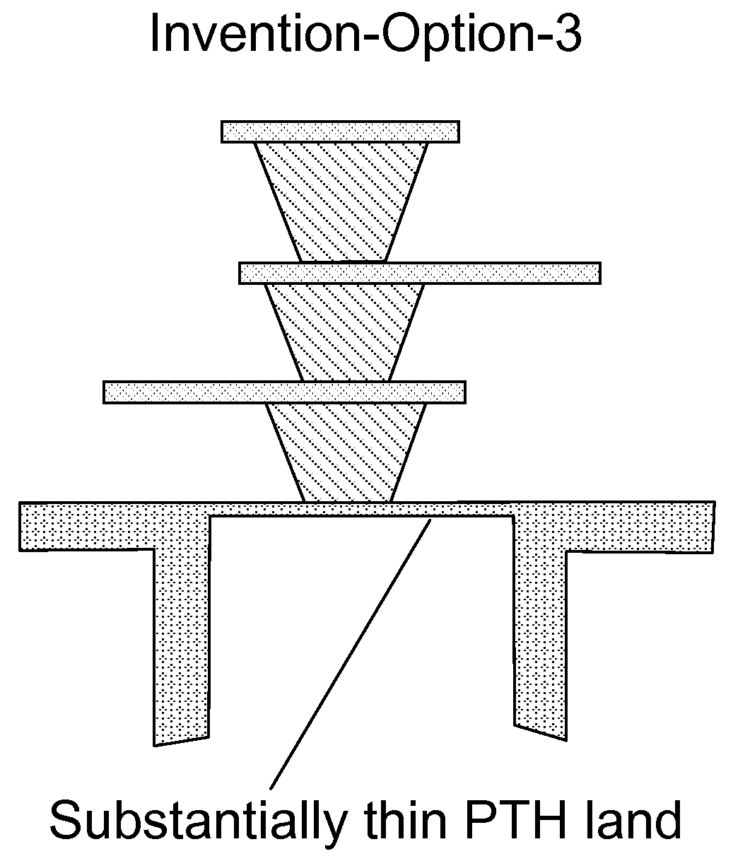
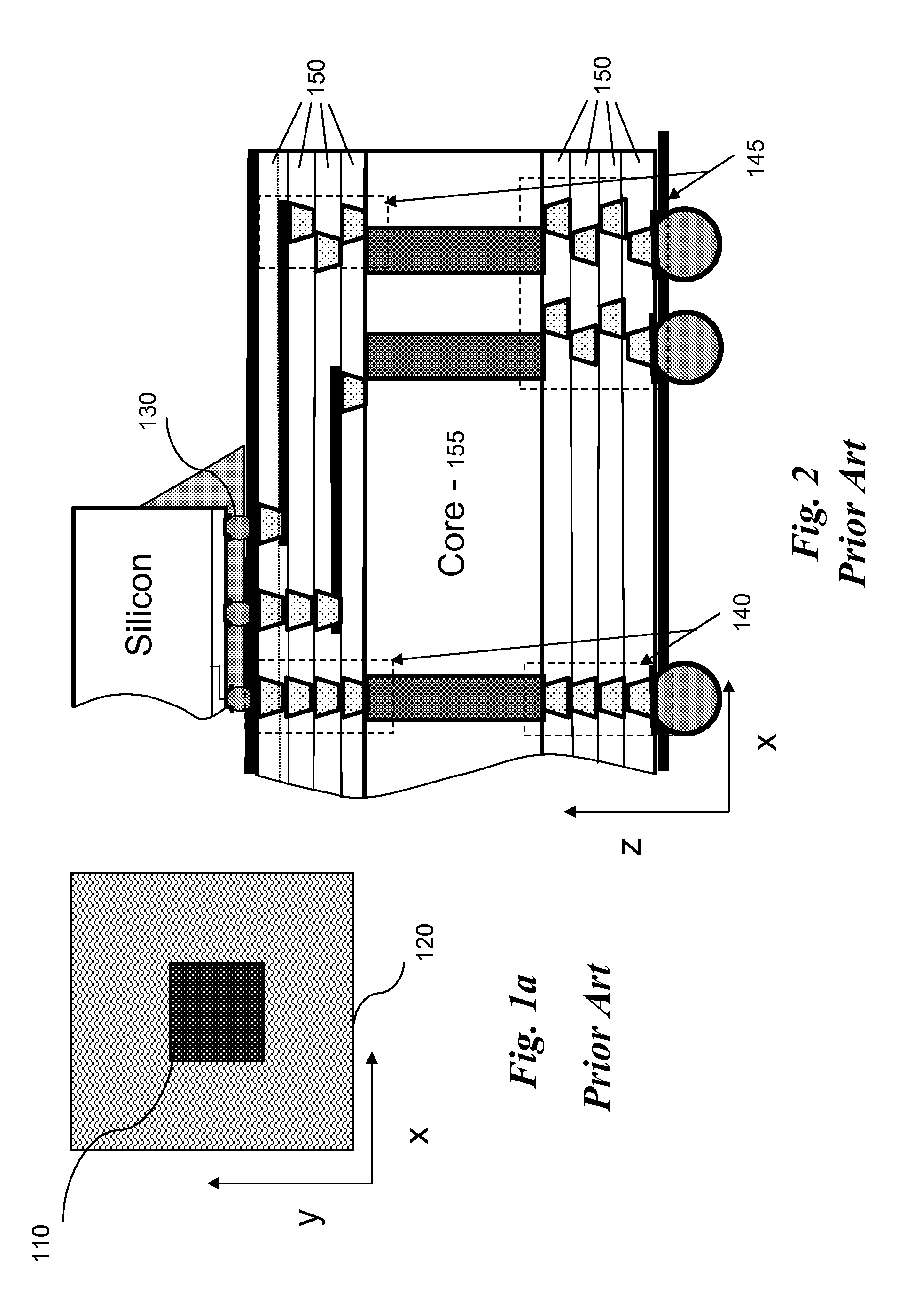
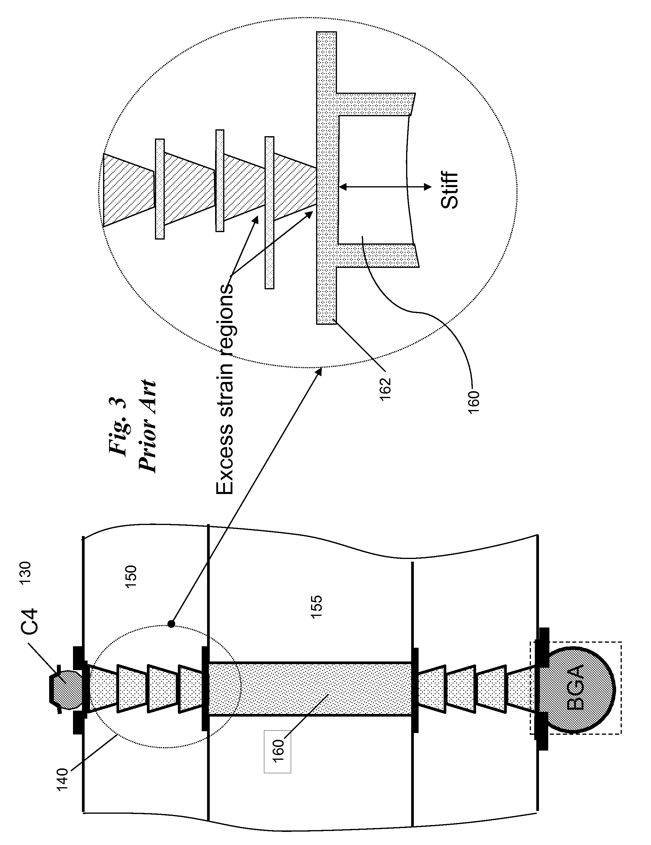
[0027]Embodiments of the present invention relate to a stacked via structure for electronic substrates such that the thermomechanical stresses on the vias are reduced. This stacked via structure reduces the vertical stiffness inherent in current via structures. Referring to FIG. 4a there is shown an optimized configuration for chip modules, according to the known art. The vias of FIG. 4a (Vial) 140 are built on the platted through hole (PTH) landing 162 and are conventionally supported by this disc-like structure, preferably made of copper (Cu). Although other materials could be used, copper is ideal because of its electrical and thermal properties.

[0028]Each via member of the three-stack via 140 is about 20 μm thick. Because of the difference in the coefficient of thermal expansion (CTE) between copper and the build-up layers 150 which occurs during a thermal cycle (125 degrees C. to −55 degrees C.), the build-up layers 150 as shown in FIG. 3 (with a CTE of approximately 20 ppm / deg...


PUM

PropertyMeasurementUnit
Thicknessaaaaaaaaaa
Thicknessaaaaaaaaaa
Angleaaaaaaaaaa

Abstract

A stacked via structure for reducing vertical stiffness includes: a plurality of stacked vias, each via disposed on a disc-like structure. The disc-like structure includes a platted through hole landing supporting the plurality of stacked vias. The platted through hole landing includes a compliant center zone; and spring-like stiffness-reducing connectors for connecting the compliant center zone of the platted through hole landing.

Description

CROSS-REFERENCE TO RELATED APPLICATIONS[0001]This application contains material similar to that disclosed in commonly-owned, co-pending applications under attorney docket numbers YOR920060721US1 and YOR920060722US1.STATEMENT REGARDING FEDERALLY SPONSORED-RESEARCH OR DEVELOPMENT[0002]None.INCORPORATION BY REFERENCE OF MATERIAL SUBMITTED ON A COMPACT DISC[0003]None.FIELD OF THE INVENTION[0004]The invention disclosed broadly relates to the field of chip design and more particularly relates to the field of electronic substrates in chip design.BACKGROUND OF THE INVENTION[0005]Integrated circuits (chips) are generally made of silicon on which electronic circuits are fabricated. These chips are placed on substrates. A substrate is made of organic materials embedded with copper interconnects. The substrate helps to join the chip to external circuits on a motherboard. FIG. 1a shows a cross-section of a chip 110 on a substrate 120. These are the two key components of an electronic module.[000...

Claims


Application Information

Patent Timeline
IPC IPC(8): H05K1/09
CPCH01L23/49827H01L23/49838H01L2224/16H01L2924/15311H05K1/0271H05K1/116Y10T29/49155H05K2201/0347H05K2201/09454H05K2201/09536H05K2201/0959H05K2201/096H05K2201/0969H05K3/4602H01L2224/05548H01L2224/05001H01L2224/05572H01L2924/00014H01L2224/05599H01L2224/05099
Inventor KACKER, KARANPOWELL, DOUGLAS O.QUESTAD, DAVID L.RUSSELL, DAVID J.SRI-JAYANTHA, SRI M.
Owner GLOBALFOUNDRIES INC
Why Eureka
Try Eureka