
Hierarchical common source line structure in NAND flash memory

a common source and line structure technology, applied in the field of nand flash memory, can solve the problems of inadvertent programming, unselected flash memory cells, and reduced vsub>dd /sub>level

Active Publication Date: 2009-06-25
MOSAID TECH
View PDF23 Cites 30 Cited by
  • Summary
  • Abstract
  • Description
  • Claims
  • Application Information

AI Technical Summary

Problems solved by technology

A problem arises when it is desired to program one flash memory cell on a word line without programming the other flash memory cells connected to the same word line.
Because the program voltage is applied to the control gate of all flash memory cells connected to a word line, an unselected flash memory cell (a flash memory cell that is not to be programmed) on the word line, especially a flash memory cell adjacent to the flash memory cell selected for programming, may become inadvertently programmed.
However, the reduction in VDD level has reduced the usefulness of the self-boosting programming method described above wherein unselected bit lines are electrically isolated.

Method used


Image

  • Hierarchical common source line structure in NAND flash memory
  • Hierarchical common source line structure in NAND flash memory
  • Hierarchical common source line structure in NAND flash memory

Examples


Embodiment Construction

[0022]In order to resolve the problem of a desired high VCC in the low power and low voltage operations of NAND flash memory, “A Source-Line Programming Scheme For Low-Voltage Operation NAND Flash Memories”, Journal of Solid State Circuits, Vol. 35 No. 5, May 2000, has been introduced by Ken Takeuchi et al. (hereinafter “Takeuchi”).

[0023]The program disturb time shown in FIG. 5 of Takeuchi is defined as when the Vth is shifted by 1.5V. The selected cell programming is done by 0V bit line and then it is programmed to have high Vth value as programmed state (logically, “0”). Therefore, the self-boosting level of the unselected cell transistor channel is very important to suppress the program disturb by the identical word line connection which have the high program voltage (see FIG. 2 of Takeuchi). However, Takeuchi didn't provide for a higher self-boosting level in the unselected cell transistor channel.

[0024]In U.S. application Ser. No. 11 / 026,825, “Source Side Asymmetrical Precharge...


PUM


Abstract

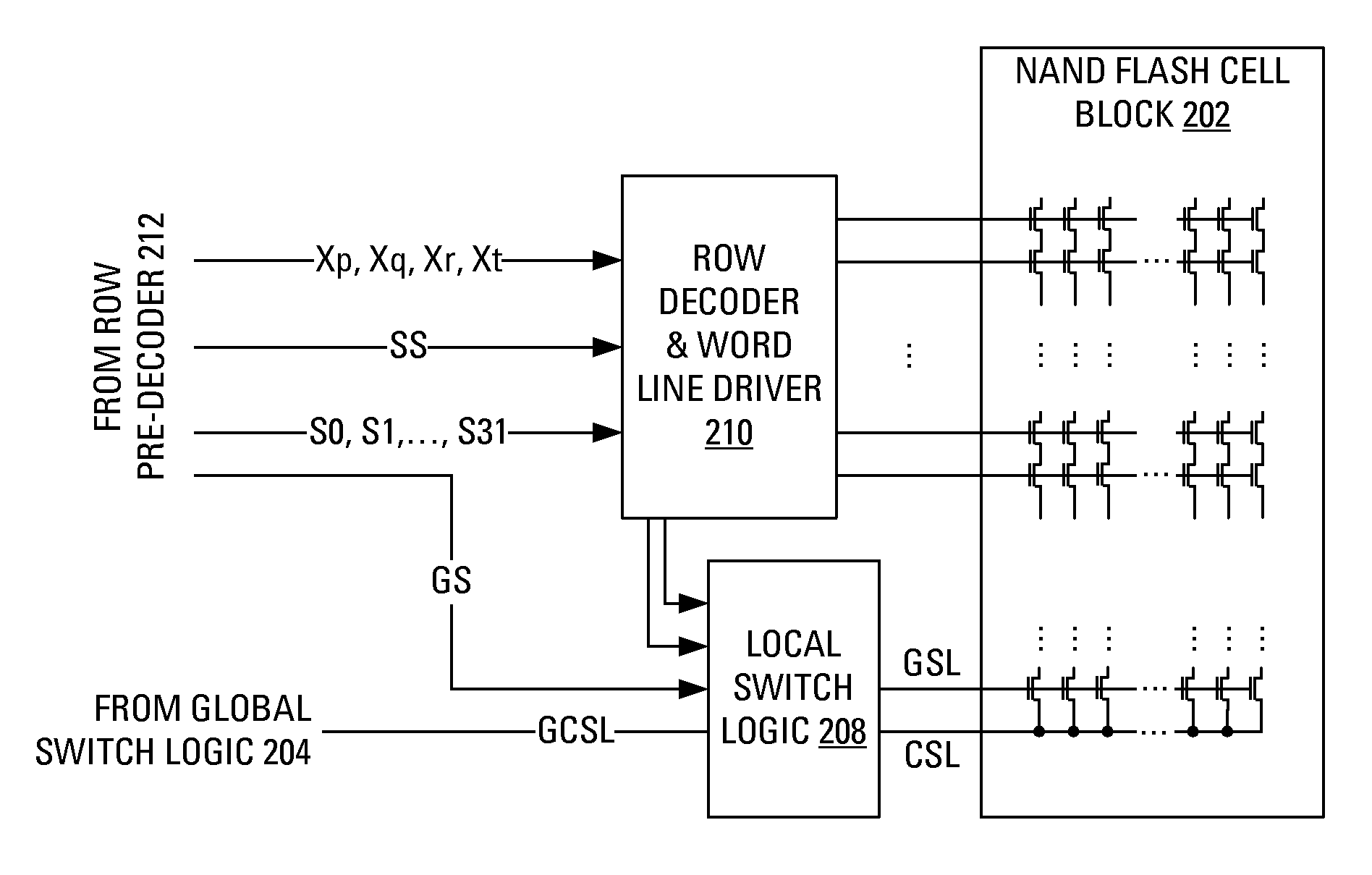
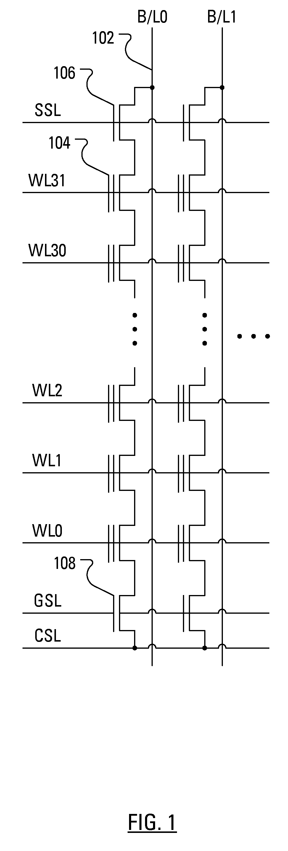
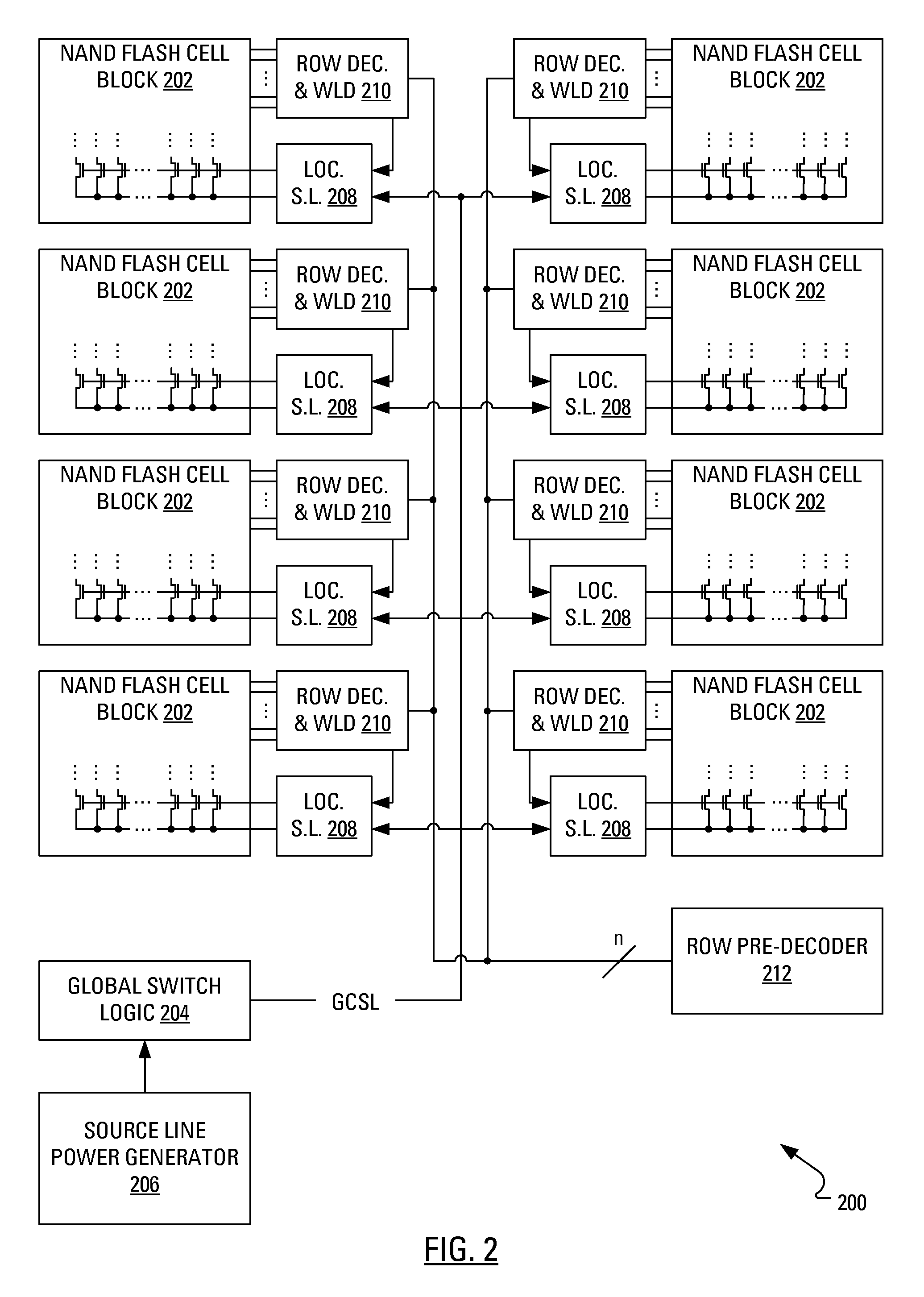
Each memory cell string in a generic NAND flash cell block connects to a Common Source Line (CLS). A value for applying to the CSL is centrally generated and distributed to a local switch logic unit corresponding to each NAND flash cell block. For source-line page programming, the distribution line may be called a Global Common Source Line (GCSL). In an array of NAND flash cell blocks, only one NAND flash cell block is selected at a time for programming. To reduce power consumption, only the selected NAND flash cell block receives a value on the CSL that is indicative of the value on the GCSL. Additionally, the CSLs of non-selected NAND flash cell blocks may be disabled through an active connection to ground.

Description

RELATED APPLICATIONS[0001]The present application claims priority from U.S. provisional Patent Application No. 61 / 015,909, filed Dec. 21, 2007, which is incorporated herein by reference in its entirety.FIELD OF THE INVENTION[0002]The present application relates generally to NAND flash memory and, more specifically, to a Hierarchical Common Source Line Structure for such memory.BACKGROUND OF THE INVENTION[0003]NAND flash memory has been proposed as a main storage element to replace hard disk drives, which have been used for a long time in the Personal Computer (PC) systems and servers. NAND flash memory uses “tunnel injection” for writing and “tunnel release” for erasing. Such writing and erasing makes use of a quantum tunneling effect, also called Fowler-Nordheim tunnel injection, wherein charge carriers are injected into an electric conductor through a thin layer of an electric insulator (a gate oxide).[0004]Recent expansion in the use of NAND flash memory in the semiconductor memo...

Claims


Application Information

Patent Timeline
Patent Type & Authority Applications(United States)
IPC IPC(8): G11C16/04G11C5/14G11C16/06
CPCG11C16/0483G11C16/3427G11C16/30G11C16/12
Inventor PYEON, HONG-BEOMKIM, JIN-KI
Owner MOSAID TECH
Learn More