Display device and electronic apparatus using the same

Active Publication Date: 2009-06-11
SEMICON ENERGY LAB CO LTD
View PDF15 Cites 21 Cited by
  • Summary
  • Abstract
  • Description
  • Claims
  • Application Information

AI Technical Summary

Benefits of technology

[0016]According to the invention having the aforementioned structures, the writing operation and the erasing operation can be performed by one gate signal line driver circuit, which results in reduced power consumption.
[0017]According to the invention having the aforementioned structures, only one gate signal line driver circuit is required; therefore, a display device with a slim bezel can be easily achieved.
[0018]According to the invention having the aforementioned structures, the gate signal line driver circuits are provided on opposite sides of the pixel portion and the same signal is supplied to a selected row from opposite sides of the row. Accordingly, a display device with high definition can be achieved even when a horizontal period is reduced and the load of a gate line is increased.

Problems solved by technology

On the other hand, the method disclosed in Patent Document 1 is disadvantageous in that a video signal is written many times in one frame period, a writing operation, an erasing operation and the like are required for controlling the light emitting time, periphery driver circuits are operated at a high frequency, and power consumption is increased.
Further, in general, a horizontal period is reduced and the load of a gate line is increased in a display device with higher definition; therefore, according to the method of inputting a signal from one side of a gate signal line, much higher definition cannot be achieved.

Method used


Image

  • Display device and electronic apparatus using the same
  • Display device and electronic apparatus using the same
  • Display device and electronic apparatus using the same

Examples


embodiment mode 1

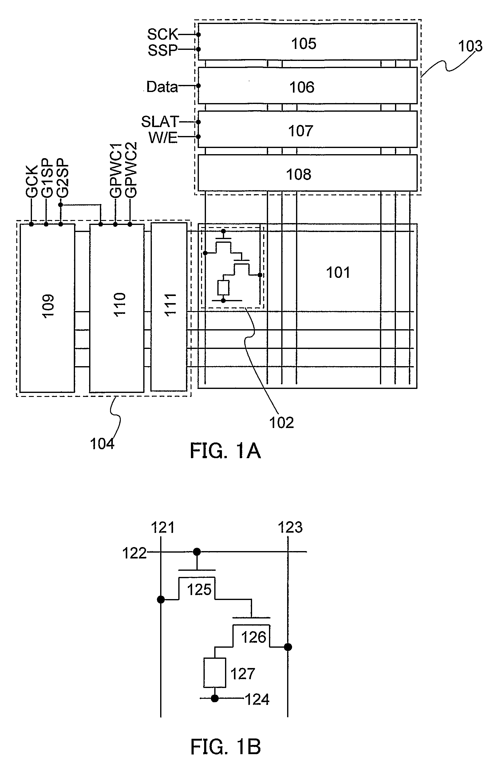
[0028]Although the invention will be described by way of Embodiment Modes and Embodiments, it is to be understood that various changes and modifications will be apparent to those skilled in the art. Therefore, unless such changes and modifications depart from the scope of the invention, they should be construed as being included therein. Described below is an example of using an RS latch as a control circuit.

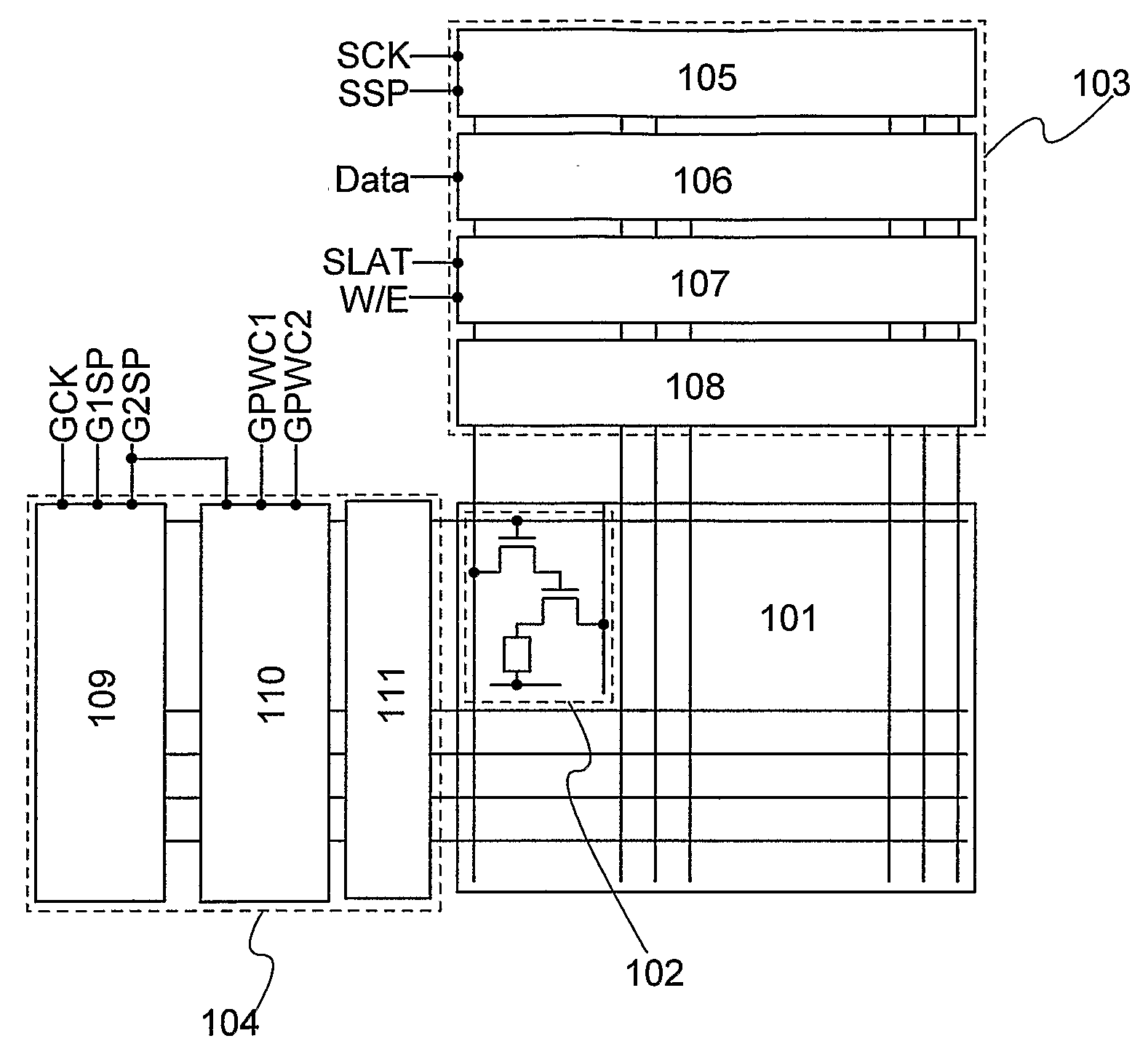
[0029]A configuration of an active matrix display device of the invention is described with reference to FIG. 1A. In a pixel portion 101, a plurality of pixels 102 each surrounded by a dotted line frame are arranged in matrix. A source driver 103 and a gate driver 104 are provided at the periphery of the pixel portion 101.

[0030]The source driver 103 has a shift register 105, a first latch circuit 106, a second latch circuit 107, and level shifter and buffer 108. The gate driver 104 has a shift register 109, an RS latch 110, and level shifter and buffer 111.

[0031]The pixel 102 is...

embodiment mode 2

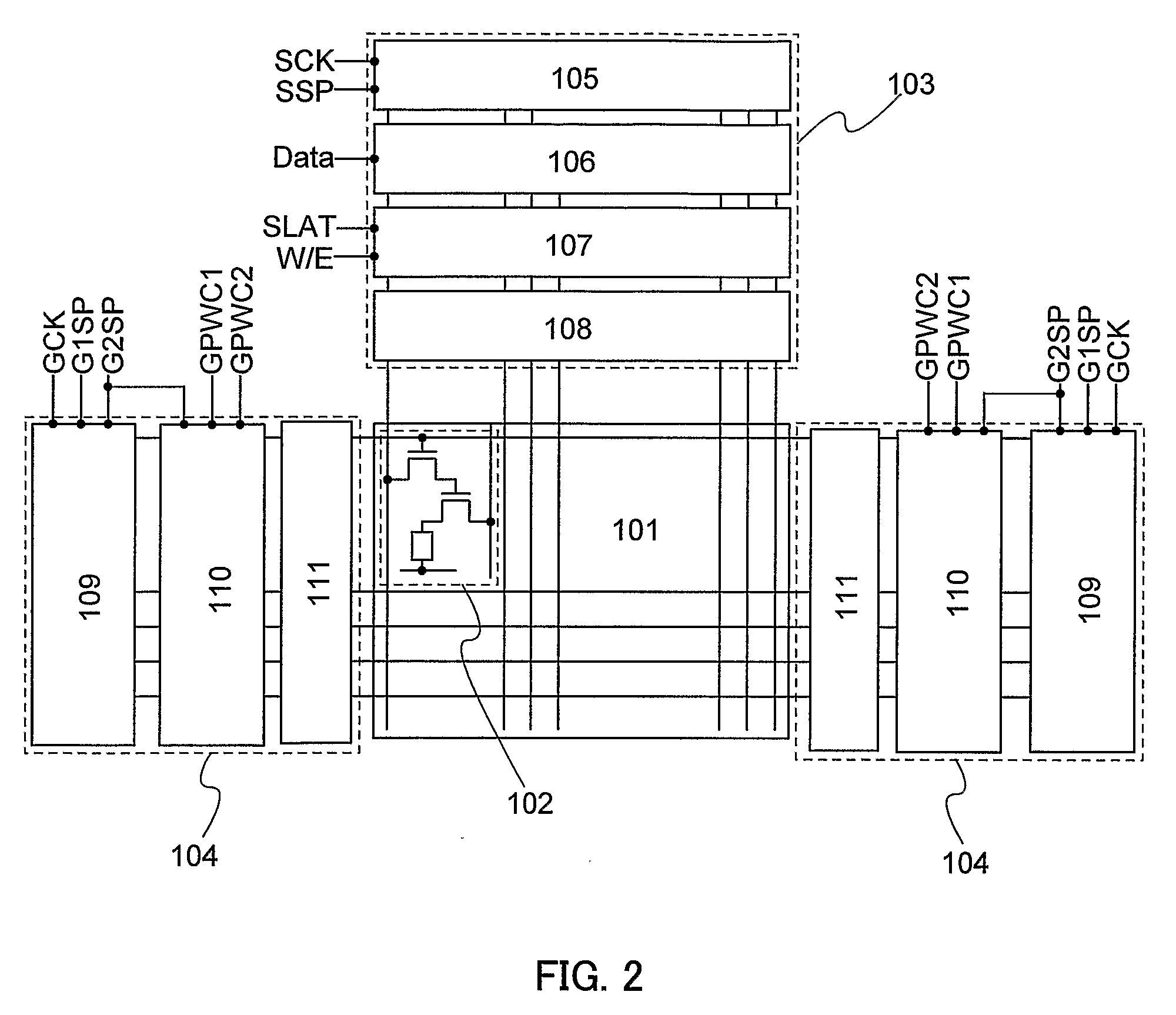
[0049]As shown in FIG. 2, when the gate drivers 104 each having the shift register 109, the RS latch 110, and the level shifter and buffer 111 are provided on opposite sides of the pixel portion 101 and the same signal is outputted from the opposite sides to the same gate signal line at a time, the signal can be transmitted to the gate signal line faster. As a result, a display device with high definition can be achieved even when a horizontal period is reduced and the load of a gate line is increased.

[0050]In FIG. 2, the identical portions to those in FIG. 1A are denoted by the identical reference numerals. The gate driver in this embodiment mode has the same configuration as that shown in FIG. 1A. This embodiment mode is different from Embodiment Mode 1 in that the gate drivers 104 are provided on opposite sides of the pixel portion 101.

embodiment mode 3

[0051]Described in this embodiment mode is a configuration example of a driver circuit of the display device of the invention, namely a source driver and a gate driver.

[0052]First, a configuration example of the source driver is described with reference to FIG. 3. The source driver has a shift register 301, a first latch circuit 302, a second latch circuit 303, a writing / erasing selection circuit 304, and a buffer circuit 305.

[0053]The shift register 301 sequentially outputs sampling pulses in accordance with clock signals (SCK, SCKb: inverted signal of SCK) and a start pulse (SSP). A video signal (Data) is sampled by the first latch circuit 302 in accordance with the sampling pulses outputted from the shift register 301. After the sampling of the video signal is completed in all the stages of the first latch circuit 302 and then latch pulses (SLAT, SLATb: inverted signal of SLAT) are inputted, the video signals held in the first latch circuit 302 are simultaneously transferred to t...


PUM


Abstract

A display device with reduced power consumption, high definition, and a slim bezel. Both of a writing operation and an erasing operation are performed by one gate driver that is mainly constituted by a shift register for selecting a row and a control circuit for switching between a writing operation and an erasing operation. The switching of the control circuit is performed using an output signal of the shift register of the row, an output signal of the control circuit of the previous row, and an externally inputted signal.

Description

TECHNICAL FIELD[0001]The present invention relates to a display device having a plurality of pixels arranged in matrix, and an electronic apparatus using the display device. More specifically, the invention relates to a display device where a video signal is inputted to a selected pixel to control each pixel and display images, and an electronic apparatus using the display device.BACKGROUND ART[0002]The demand for dot matrix display devices typified by liquid crystal display devices has been rapidly increasing for portable applications as well as fixed applications such as a TV receiver and a display for a personal computer. In recent years, as a next-generation display device replacing liquid crystal display devices, EL display devices that have pixels each including an organic electroluminescence (EL) element have been put into practical use.[0003]A dot matrix display device is generally classified into a passive matrix display device and an active matrix display device. In the ac...

Claims


Application Information

Patent Timeline
IPC IPC(8): G09G3/20
CPCG09G3/2037G09G3/3677G11C19/28G09G2310/0267G09G2310/061G09G2310/0205G09G3/30G09G3/32G09G3/20H05B33/12
Inventor MIYAKE, HIROYUKI
Owner SEMICON ENERGY LAB CO LTD
Why Eureka
Try Eureka