
Method for manufacturing semiconductor device

Inactive Publication Date: 2009-05-28
LAPIS SEMICON CO LTD
View PDF2 Cites 12 Cited by
  • Summary
  • Abstract
  • Description
  • Claims
  • Application Information

AI Technical Summary

Benefits of technology

[0013]An object of the present invention is to provide a method for manufacturing a semiconductor device that can promise sufficient alignment precision while reducing a manufacturing cost of the semiconductor device.
[0015]The semiconductor device manufacturing method according to the present invention does not have unnecessary photolithography and etching processes. This decreases a production cost, and ensures excellent alignment precision.

Problems solved by technology

Therefore, deterioration of alignment precision occurs.

Method used


Image

  • Method for manufacturing semiconductor device
  • Method for manufacturing semiconductor device
  • Method for manufacturing semiconductor device

Examples


embodiment 1

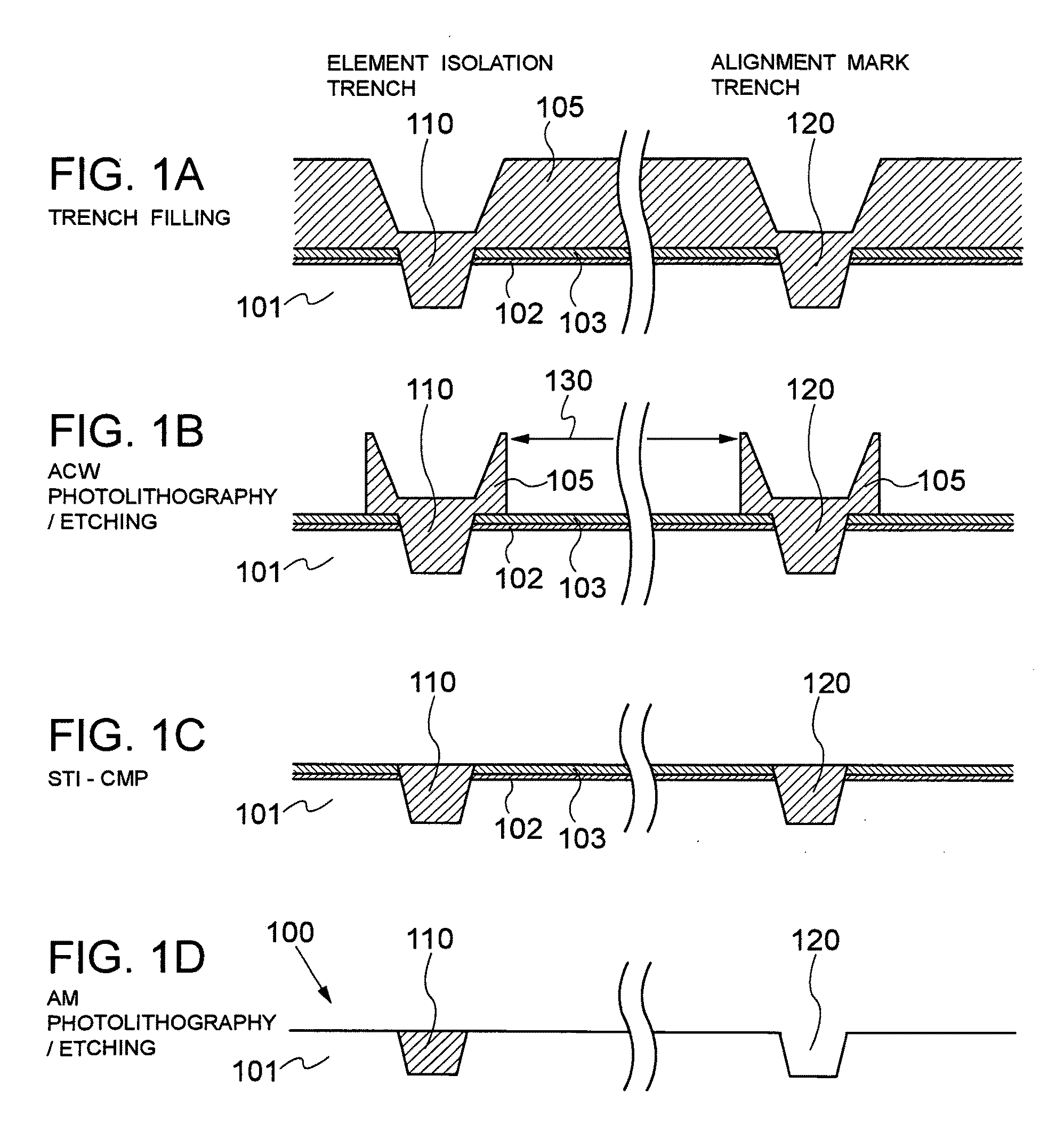
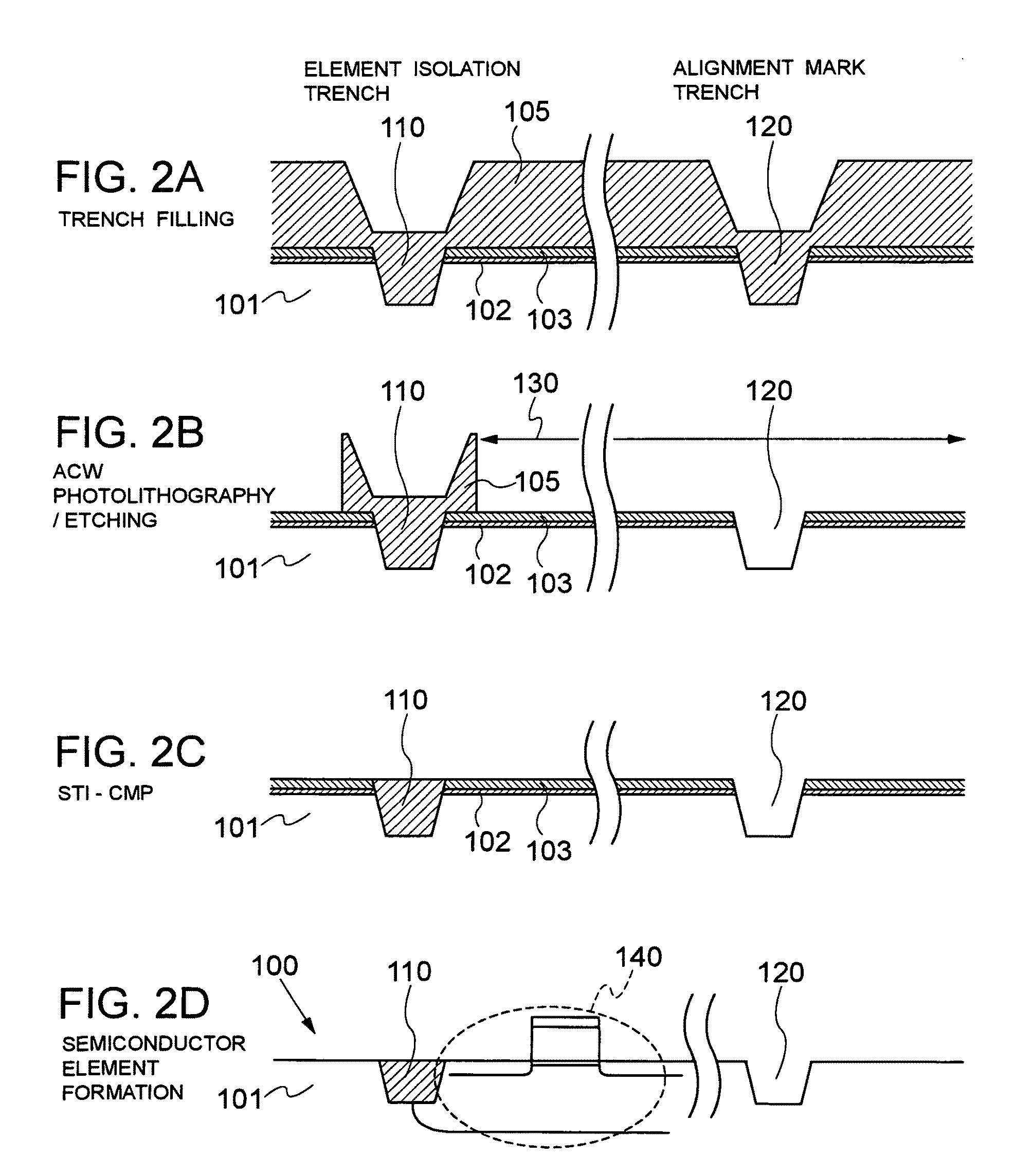
[0024]This embodiment is illustrated in FIGS. 2A to 2D. These drawings are schematic views showing a method for manufacturing a semiconductor device according to one exemplary embodiment of the present invention. The semiconductor device to be manufactured includes trenches for element separation (isolation) to divide an active region on a substrate into a plurality of individual active regions. In each individual active region, a semiconductor element such as a MOS transistor is formed. The element separation (isolation) trenches are used to separate (isolate) the individual active regions from each other. The semiconductor device also includes another trenches for alignment mark. The alignment mark trenches are formed along grid lines to define an arrangement of semiconductor elements.

[0025]In a process of filling a trench as shown in FIG. 2A, a pad oxide film 102 and a silicon nitride film 103 are formed in this order on a surface of a silicon substrate 101, followed by a photoli...

embodiment 2

[0032]Embodiment 2 is a modification to Embodiment 1. In Embodiment 1, a certain amount of foreign matters may be produced during the CMP process, and such foreign matters may remain in the alignment mark trenches. Embodiment 2 deals with this problem by using a sacrifice oxide film. In the ACW photolithography / etching process of Embodiment 2, the oxide film deposited in the alignment mark trenches is completely removed, and then the sacrificial oxide film is formed over the entire wafer including the alignment mark trenches, so as to eliminate foreign materials.

[0033]FIG. 4A is an enlarged SEM photograph showing an alignment mark part and FIG. 4B is a (virtual) cross-sectional view of the alignment mark part. Referring to FIG. 4A, a trench (TR) hole is shown in a 50K enlarged image. Some foreign materials are found in the trench. Three white circles in FIG. 4A show the locations of the foreign materials. The trench has two side walls. Referring to FIG. 4B, the foreign materials whi...


PUM


Abstract

A method for manufacturing a semiconductor device includes forming a plurality of trenches for element isolation and a plurality of trenches for alignment mark on a substrate. The substrate has an active region. The method also includes laminating an oxide film on the substrate and over both of the trenches. The method also includes etching the oxide film using a resist mask that masks the element isolation trenches, so that the oxide film laminated in the active region and the oxide film laminated in the alignment mark trenches are removed. The method also includes polishing a surface of the substrate to planarize or smooth the surface of the substrate. Accordingly, those portions of the oxide film which project from the substrate surface are eliminated and the oxide film remains only inside the element isolation trenches. This divides the active region into a plurality of individual active regions for the respective semiconductor elements. The method also includes positioning the resist mask using the alignment mark trenches. The resist mask is used to fabricate the semiconductor elements in the active regions of the substrate.

Description

BACKGROUND OF THE INVENTION[0001]1. Field of the Invention[0002]The present invention relates to a method for manufacturing a semiconductor device, and in particular, to a method for manufacturing a semiconductor device which forms semiconductor elements in an active element separation region (hereinafter referred to as “active region”) on a semiconductor substrate.[0003]2. Description of the Related Art[0004]With recent progress in integration density and functions of semiconductor devices, there is a demand for smaller element separation regions for isolating many (or more) semiconductor elements such as MOS transistors. A shallow trench isolation (hereinafter referred to as “STI”) process is drawing an attention as an effective technology for providing fine element isolation (separation) regions.[0005]The STI process is a technique that forms a groove (hereinafter referred to as “trench”) on a semiconductor substrate by etching and fills the trench with an insulating material so ...

Claims


Application Information

Patent Timeline
IPC IPC(8): H01L21/762
CPCH01L21/823481H01L21/76224Y10S438/975
Inventor NARITA, TADASHIOSHIMA, KATSUO
Owner LAPIS SEMICON CO LTD
Learn More