Integrated circuit package
a technology of integrated circuits and components, applied in the direction of solid-state devices, electric devices, basic electric elements, etc., can solve the problems of limited possible interaction between sensors and media, and the design freedom is very limited, and achieves the effect of good basis for proper positioning
- Summary
- Abstract
- Description
- Claims
- Application Information
AI Technical Summary
Benefits of technology
Problems solved by technology
Method used
Image
Examples
second embodiment
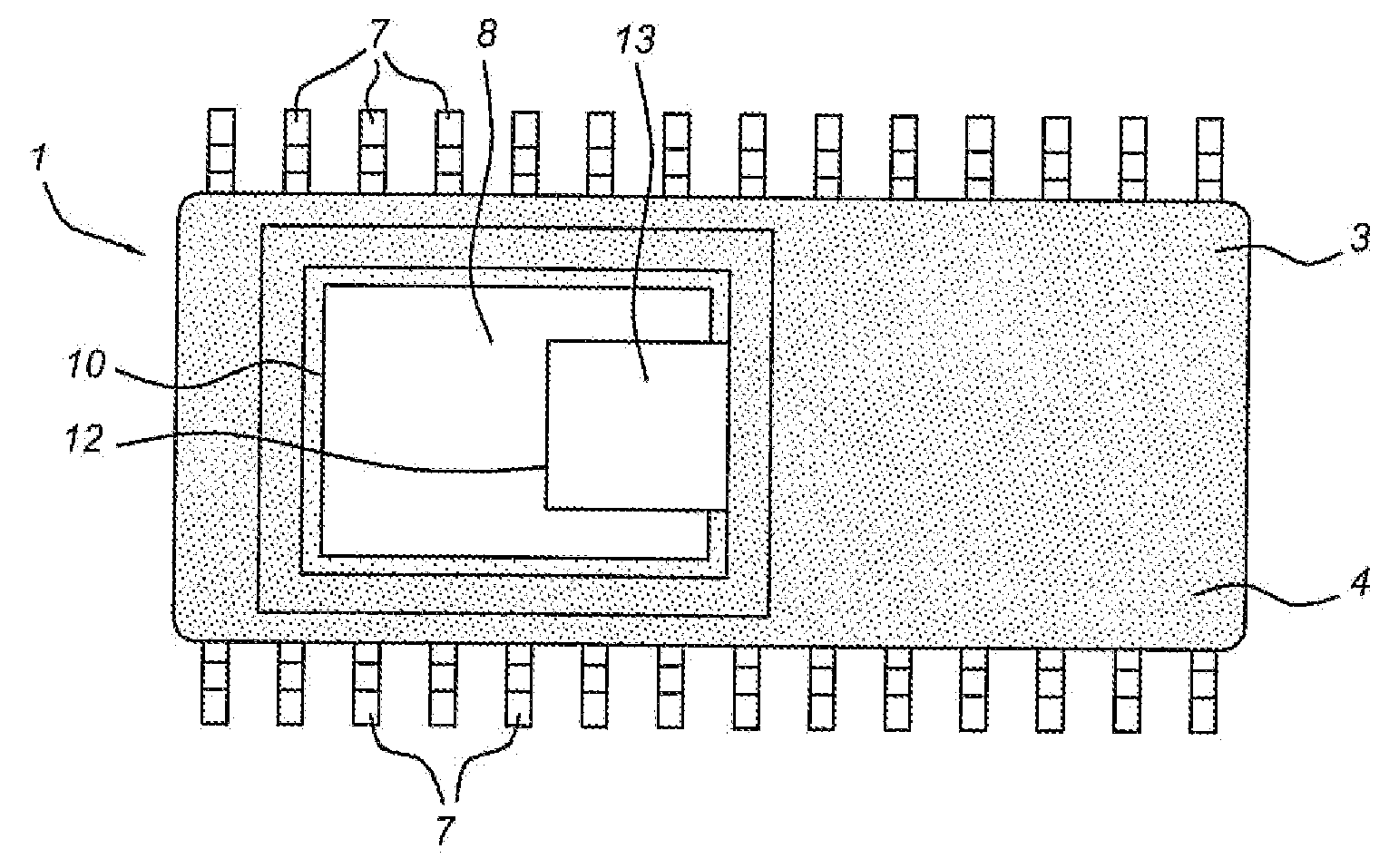
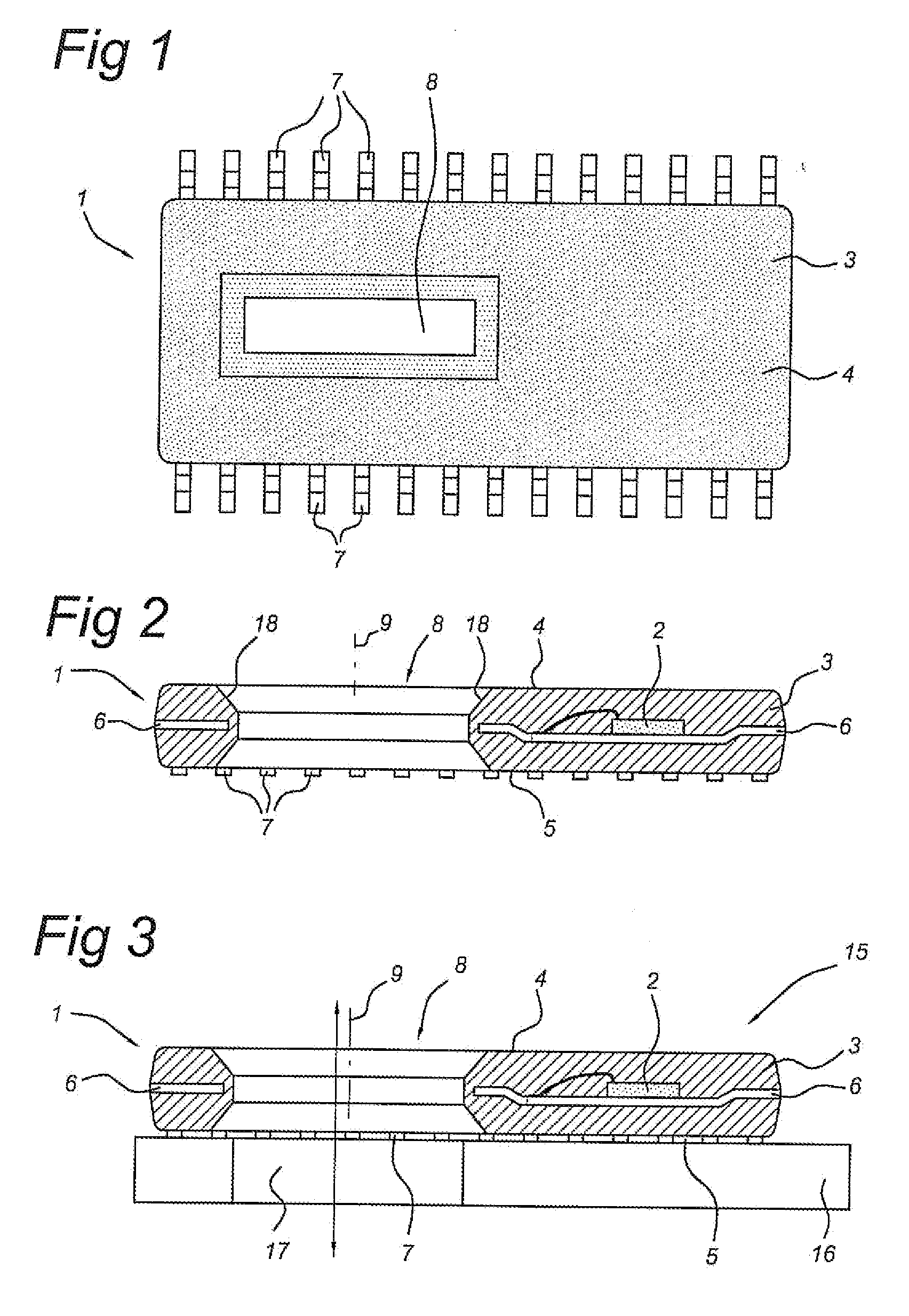
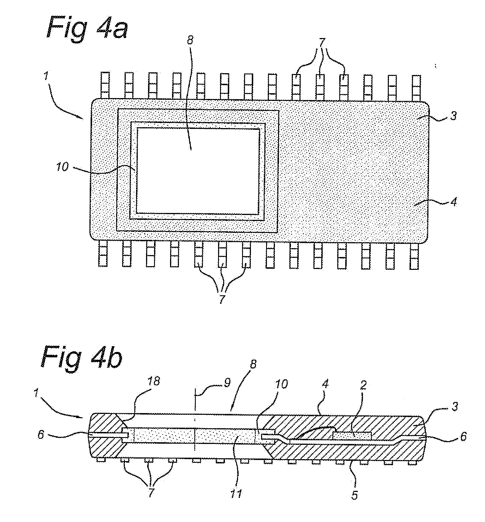
[0038]In FIG. 4a and 4b the package according to the invention is shown. The package 1 for protecting an IC 2 comprises a housing 3 having two major surfaces 4, 5 which are substantially plan parallel to each other. The housing 3 contains a lead frame 6. This lead frame 6 carries the IC 2 and any other desired component. Contact pads of the IC 2 are electrically connected to the lead frame 6 by e.g. wire-bonding. Outside contact terminals 7 are electrically connected via the lead frame 6 with the IC 2. Extremities of contact terminals 7 all lie in a plane substantially parallel to the major surfaces 4, 5. The package 1 is provided with a through-hole 8 with a rectangular shape. Other shapes are possible for the through-hole like a circle, oval square etc. At the outline of the through-hole 8, a chamfer 18 is provided. This chamfer 18 simplifies fitting e.g. a tube in the through-hole 8. The package 1 is further provided with a ring member 10 arranged in through-hole 8. The shape of ...
third embodiment
[0039]FIG. 5a-5b and FIG. 6 show the package according to the invention. The package 1 for protecting an IC 2 comprises a housing 3 having two major surfaces 4, 5 which are substantially plan parallel to each other. The housing 3 contains a lead frame 6. This lead frame 6 carries the IC 2 and any other desired component. Contact pads of the IC 2 are electrically connected to the lead frame 6 by e.g. wire-bonding. Outside contact terminals 7 are electrically connected via the lead frame 6 with the IC 2. Extremities of contact terminals 7 all lie in a plane substantially parallel to the major surfaces 4, 5. The package 1 is provided with a through-hole 8 with a rectangular shape. Other shapes are possible for the through-hole like a circle, oval square etc. At the outline of the through-hole 8, a chamfer 18 is provided. This chamfer 18 simplifies fitting e.g. a tube in the through-hole 8. The package 1 is further provided with a ring member 10 arranged in through-hole 8. The shape of ...
PUM
 Abstract
Description
Claims
Application Information
 - R&D
- Intellectual Property
- Life Sciences
- Materials
- Tech Scout
- Unparalleled Data Quality
- Higher Quality Content
- 60% Fewer Hallucinations
Browse by: Latest US Patents, China's latest patents, Technical Efficacy Thesaurus, Application Domain, Technology Topic, Popular Technical Reports.
© 2025 PatSnap. All rights reserved.Legal|Privacy policy|Modern Slavery Act Transparency Statement|Sitemap|About US| Contact US: help@patsnap.com


