Microprocessor common-mode emissions reduction circuit

Inactive Publication Date: 2009-03-05
DELPHI TECH INC
View PDF12 Cites 7 Cited by
  • Summary
  • Abstract
  • Description
  • Claims
  • Application Information

AI Technical Summary

Benefits of technology

[0007]The present invention is directed to an apparatus for significantly reducing radiated RF emissions from an integrated circuit, such as a microprocessor, having a switching characteristic giving rise to the production of common-mode RF switching currents. If left uncontrolled, such currents can produce RF emissions The use of the present invention, however, can realize a 10-15 dB improvement (i.e., a reduction) in such common-mode RF emissions.
[0008]An apparatus having reduced common-mode RF emissions arising from operation of a switching device, for example a microprocessor, includes a circuit board, first and second capacitors and a common-mode (CM) choke. The circuit board has a connector configured for connection to an external wire harness, which may otherwise operate, in the absence of the present invention, as an antenna for generating RF emissions. In a preferred embodiment, the microprocessor is of the type that includes a power pin (VCC), a ground pin (VSS), and at least one high impedance input pin. The first capacitor is a decoupling capacitor and is connected across the power and ground pins of the microprocessor (i.e., as close as possible). The second capacitor is connected across the high impedance input pin and the ground pin of the microprocessor (i.e., again as close as possible). The common-mode (CM) choke is electrically intermediate the power and ground pins of the microprocessor, on the one hand, and corresponding power and ground terminals of the connector, on the other hand. The choke is operative to substantially cancel the common mode RF currents thereby reducing common mode RF emissions.
[0009]The CM choke is disposed a preselected distance from the microprocessor, preferably as physically close as possible. This close proximity is configured to achieve an effective level of common-mode RF emissions. The positioning of the CM choke improves the canceling effect as to the CM currents before significant emissions results. Additionally, the invention includes an isolation feature, which ensures effective control of the CM RF emissions. In this regard, the power and ground terminals of the connector are coupled to corresponding electrically conductive first traces disposed on the circuit board. The power and ground pins of the microprocessor are coupled to electrically conductive second traces disposed on the circuit board. The first traces are located outside a predefined isolation zone surrounding the second traces associated with the microprocessor. In a preferred embodiment, the isolation zone is configured in size and shape so as to substantially minimize capacitive coupling from the second traces to the first traces.

Problems solved by technology

Electromagnetic interference (EMI) and radio frequency (RF) interference can be in general a significant problem for many electrical circuits.
This problem has become more challenging to manage effectively as the use of electronics in all variety of products expands.
Thus, while some approaches have been somewhat effective in reducing common-mode RF emissions, meeting OEM test requirements continues to present challenges.

Method used


Image

  • Microprocessor common-mode emissions reduction circuit
  • Microprocessor common-mode emissions reduction circuit
  • Microprocessor common-mode emissions reduction circuit

Examples


Embodiment Construction

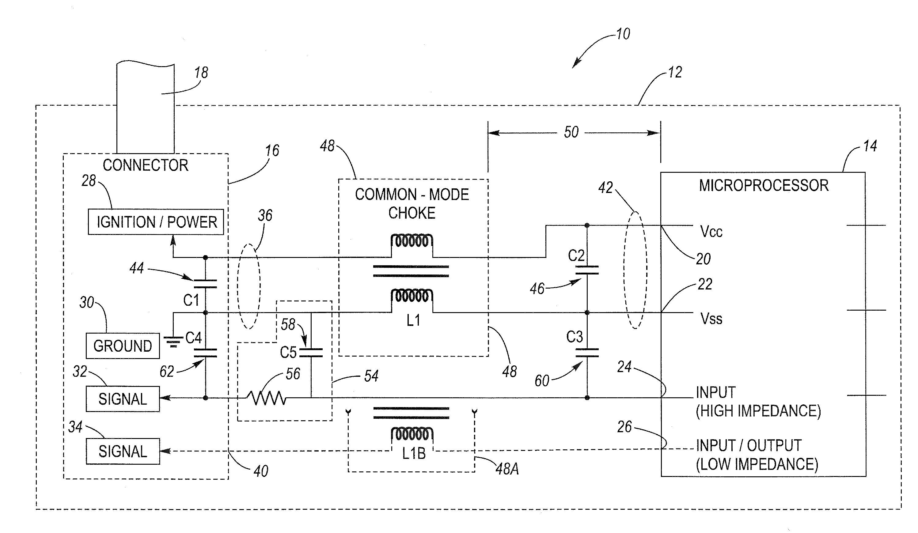
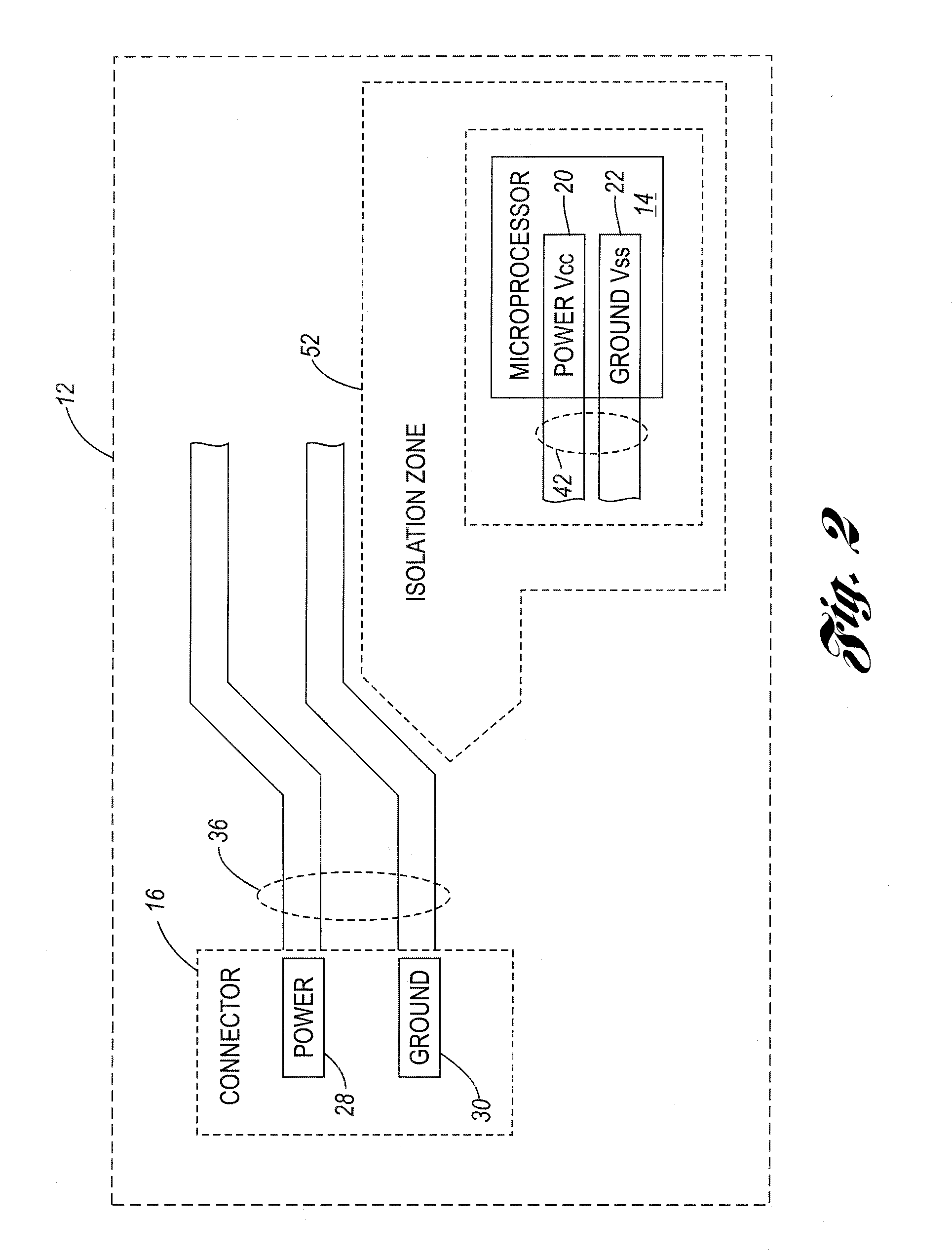
[0014]Referring now to the drawings, wherein like reference numerals are used to identify identical components in the various views, FIG. 1 is a schematic and block diagram of an electronic apparatus 10 including common-mode (CM) RF emissions reduction features according to the present invention. Apparatus 10 includes a main circuit board 12 on which is disposed an integrated circuit having electrical switching characteristics, such as a microprocessor 14, that is susceptible to producing CM RF currents, and hence CM RF emissions. FIG. 1 additionally shows circuit board 12 having a connector 16 located thereon configured for connection to an external wire harness 18 or the like. As described above, the present invention is directed to minimizing or eliminating RFI by addressing a principal source of such emissions, namely, microprocessor RF emissions. As to microprocessor RF emissions, the primary source involves common-mode (CM) RF currents. As one example, such CM RF currents occu...


PUM


Abstract

An apparatus with reduced common-mode (CM) emissions from of a microprocessor includes a circuit board, first and second capacitors and a common-mode (CM) choke. The circuit board has a connector configured for connection to an external wire harness, which may act as an antenna generating CM RF emissions. The microprocessor includes a power pin (VCC), a ground pin (VSS), and at least one high impedance input pin. The first capacitor is connected across the power and ground pins. The second capacitor is connected across the high impedance input pin and the ground pin. The common-mode (CM) choke is electrically intermediate the power and ground pins, on the one hand, and the corresponding power and ground terminals of the connector on the other hand. The CM choke is disposed a preselected distance from the microprocessor. The preselected distance, which may be as close as possible, is configured to achieve an effective amount of common-mode emissions attenuation. The power and ground terminals are coupled to electrically conductive first traces on the circuit board, while the power and ground pins are coupled to electrically conductive second traces on the circuit board. The first traces are located outside a predefined isolation zone surrounding the second traces. The isolation zone is configured in size and shape so as to substantially minimize capacitive coupling between the second traces and the first traces.

Description

TECHNICAL FIELD[0001]The present invention relates to a microprocessor common-mode (CM) emissions reduction circuit.BACKGROUND OF THE INVENTION[0002]Electromagnetic interference (EMI) and radio frequency (RF) interference can be in general a significant problem for many electrical circuits. This problem has become more challenging to manage effectively as the use of electronics in all variety of products expands. An entire discipline has developed to address such problems, and a correspondingly wide variety of strategies and / or products have been developed, as seen for example by reference to U.S. Pat. No. 6,346,865 issued to Callewaert et al. entitled “EMI / RFI FILTER INCLUDING A FERROELECTRIC / FERROMAGNETIC COMPOSITE”, assigned to the common assignee of the present invention, and hereby incorporated by reference herein in its entirety.[0003]In particular, in the automotive field, most if not all original equipment manufacturers (OEM) of trucks and automobiles require that electronic...

Claims


Application Information

Patent Timeline
IPC IPC(8): H03H1/00
CPCH05K1/0231H05K1/0233H05K2201/1003H03H1/0007H05K2201/10189H05K2201/10689H03H7/427H05K2201/1006
Inventor PAKKALA, WILLIAM F.
Owner DELPHI TECH INC
Why Eureka
Try Eureka