Power layout of integrated circuits and designing method thereof
- Summary
- Abstract
- Description
- Claims
- Application Information
AI Technical Summary
Benefits of technology
Problems solved by technology
Method used
Image

Examples
Embodiment Construction
[0021]The characteristic, spirit, advantage, and convenience in practice of the invention can be particularly explained by the following preferred embodiments according to the invention.
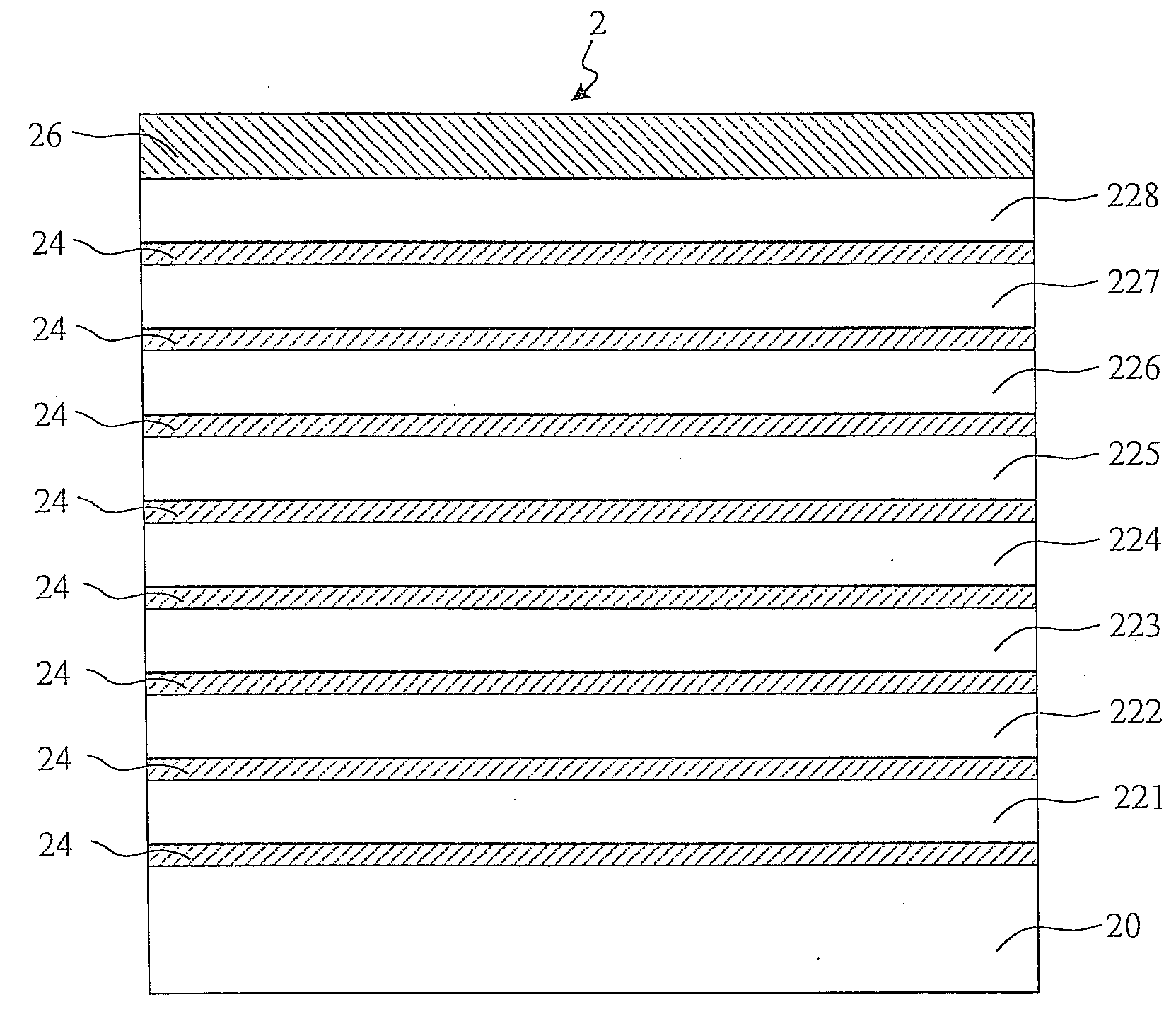
[0022]Please refer to FIG. 2A. FIG. 2A shows a simplified sectional view of an IC die (or a chip) 2 in a preferred embodiment according to the invention. As shown in FIG. 2A, the IC die 2 includes a semiconductor layer 20, eight successive metal layers (221˜228) from bottom to top, several insulating layers 24 formed between two adjacent metal layers respectively, and a passivation layer 26. The semiconductor layer 20 is used for forming electronic components such as transistors (not shown in FIG. 2A). The number of the metal layers is determined by the complexity of the practical routing. Thus, the eight metal layers shown in FIG. 2A are provided only for the convenience of explanation, not as a limit to the invention.
[0023]Regarding the routing at the metal layers 221˜228, a power distribution netw...
PUM
 Abstract
Description
Claims
Application Information
 - R&D Engineer
- R&D Manager
- IP Professional
- Industry Leading Data Capabilities
- Powerful AI technology
- Patent DNA Extraction
Browse by: Latest US Patents, China's latest patents, Technical Efficacy Thesaurus, Application Domain, Technology Topic.
© 2024 PatSnap. All rights reserved.Legal|Privacy policy|Modern Slavery Act Transparency Statement|Sitemap