Package and the method for making the same, and a stacked package
- Summary
- Abstract
- Description
- Claims
- Application Information
AI Technical Summary
Benefits of technology
Problems solved by technology
Method used
Image
Examples
Embodiment Construction
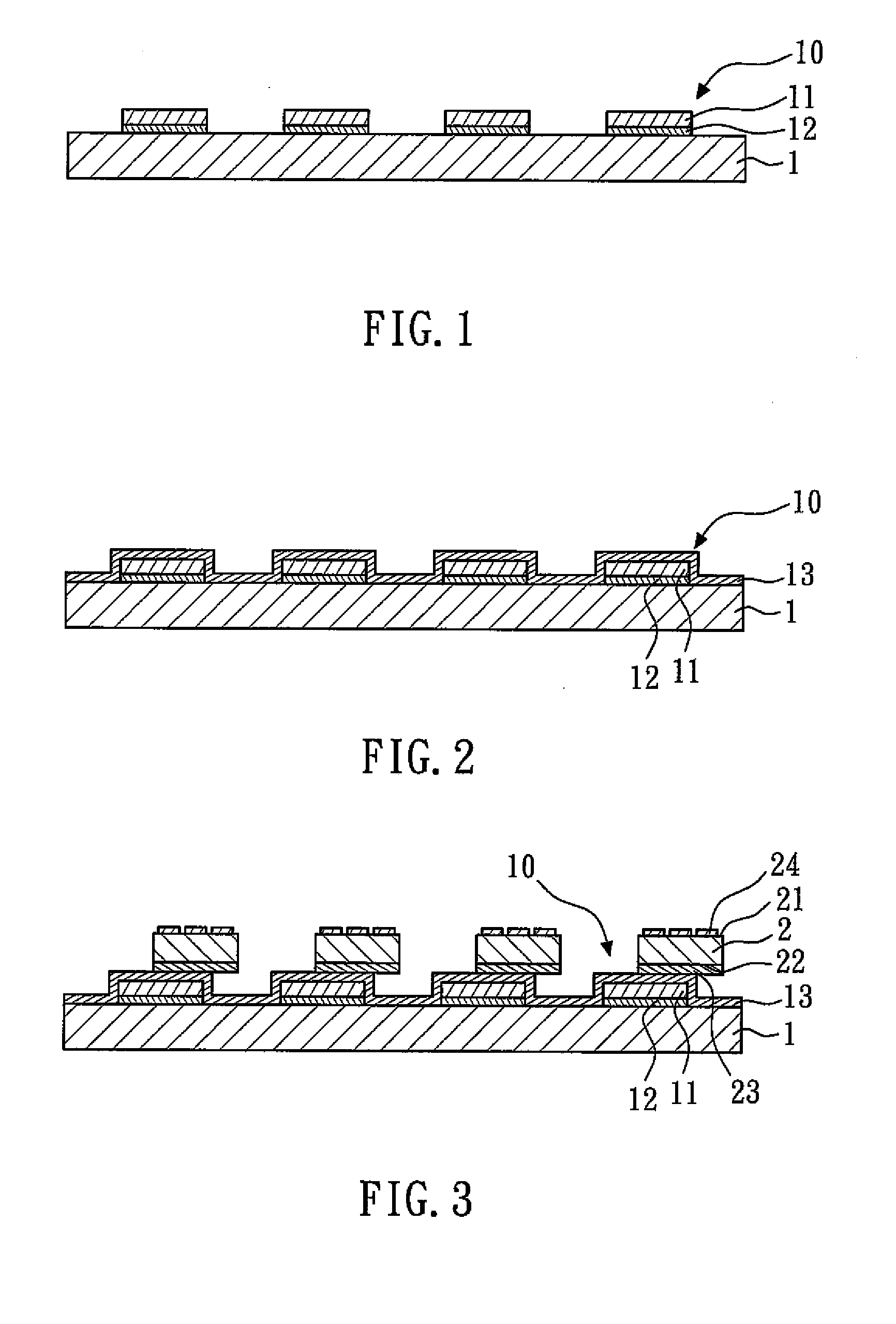
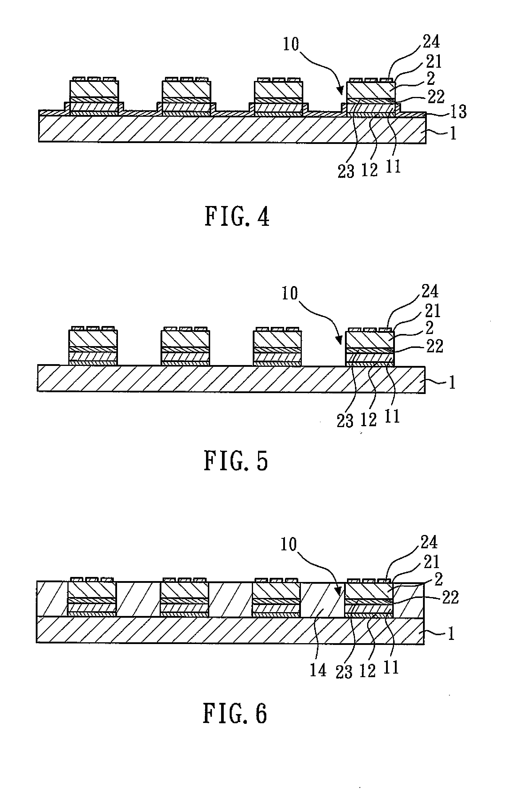
[0010]FIGS. 1 to 10 show the schematic views of the method for making the package according to the present invention. First, as shown in FIG. 1, a carrier 1 is provided. The carrier 1 has a plurality of platforms 10. In the embodiment, the carrier 1 is a silicon wafer, and each of the platforms 10 comprises a solder layer 11 and a pad 12. The pad 12 is disposed between the solder layer 11 and the carrier 1, and the material of the pad 12 is preferably metal.
[0011]As shown in FIG. 2, a flux 13 is formed on the platforms 10 and the carrier 1.
[0012]As shown in FIG. 3, a plurality of dice 2 are provided, and disposed on the platforms 10, that is, on the flux 13. In the embodiment, the dice 2 are tested and are known good dice. Each of the dice 2 comprises a first surface 21 and a second surface 22. The second surface 22 faces the platforms 10, and the second surface 22 further comprises a wettable layer 23. The first surface 21 further comprises a plurality of ball pads 24.
[0013]As show...
PUM
 Abstract
Description
Claims
Application Information
 - R&D
- Intellectual Property
- Life Sciences
- Materials
- Tech Scout
- Unparalleled Data Quality
- Higher Quality Content
- 60% Fewer Hallucinations
Browse by: Latest US Patents, China's latest patents, Technical Efficacy Thesaurus, Application Domain, Technology Topic, Popular Technical Reports.
© 2025 PatSnap. All rights reserved.Legal|Privacy policy|Modern Slavery Act Transparency Statement|Sitemap|About US| Contact US: help@patsnap.com


