Solid state image sensor

Inactive Publication Date: 2009-02-12
COLLABO INNOVATIONS INC
View PDF3 Cites 4 Cited by
  • Summary
  • Abstract
  • Description
  • Claims
  • Application Information

AI Technical Summary

Benefits of technology

[0016]In order to solve the conventional problems, it is an object of the present invention to provide a solid state image sensor capable of improving transfer efficiency, increasing the number of saturated electrons and reducing transfer efficiency variations and saturation variations.

Problems solved by technology

Therefore, the gate length of the outlet and the width of the CCD cannot be reduced and the number of saturated electrons at the horizontal CCD outlet cannot be maintained, and it is therefore difficult to improve transfers at the outlet for the purpose of increasing the speed of horizontal CCD drive.
However, since this technique forms a CCD channel so as to have a higher concentration and shallower structure, potential variations occur only locally during a transfer, the transfer electric field in the entire channel attenuates and transfer deterioration at the horizontal CCD outlet becomes more noticeable.
For this reason, with micro cells of 2.0 μm or less in a CCD solid state image sensing element, characteristics such as the number of saturated electrons and horizontal transfer efficiency at the horizontal outlet become dominant and it is difficult to realize high-speed horizontal driving while maintaining a high number of saturated electrons.
Especially, it is difficult to realize high-speed driving.
For this reason, this structure is liable to cause deterioration of a transfer from right below the offset gate electrode which is the end of the horizontal outlet to the FD section.

Method used


Image

  • Solid state image sensor
  • Solid state image sensor
  • Solid state image sensor

Examples


embodiment 1

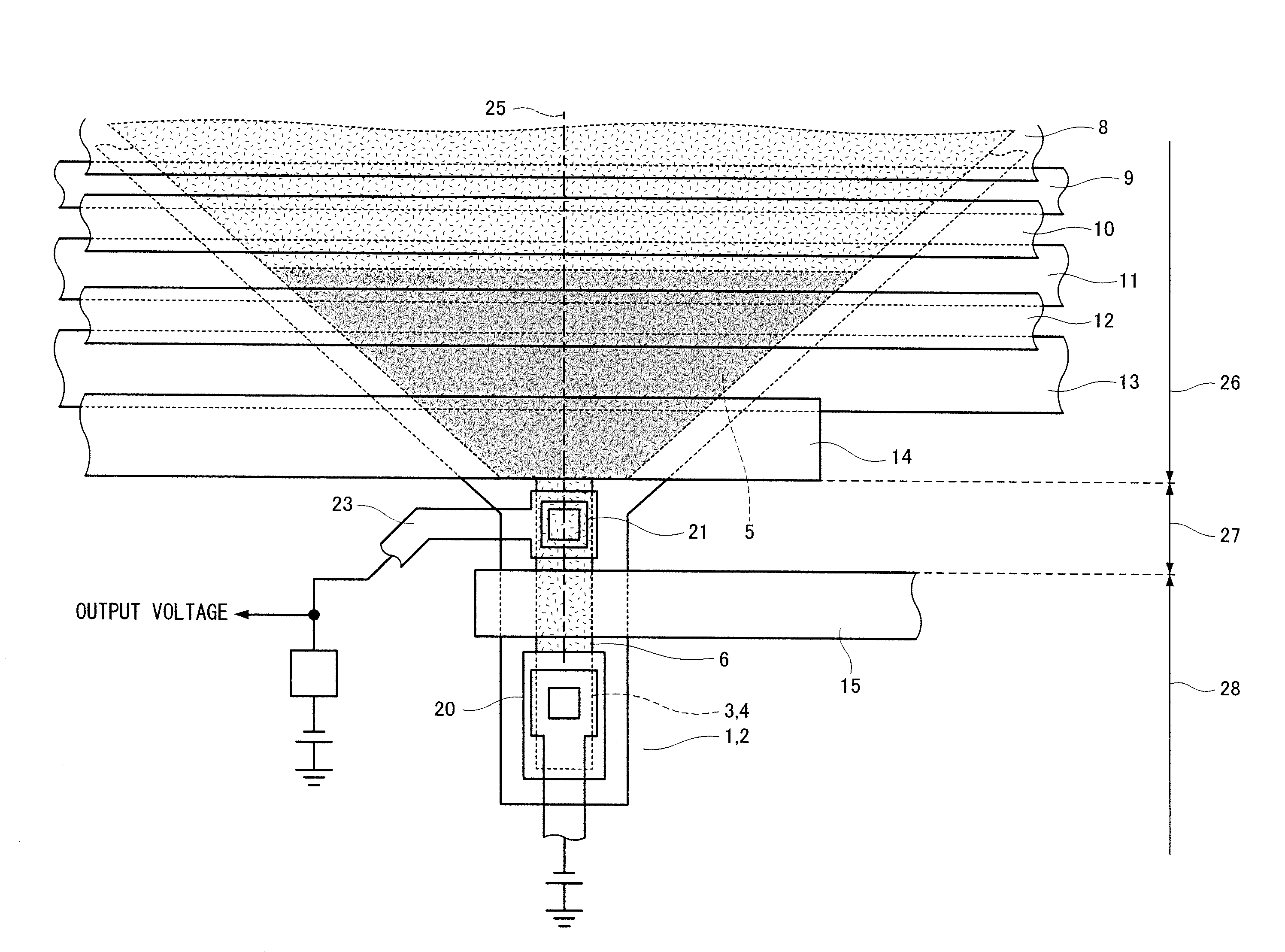
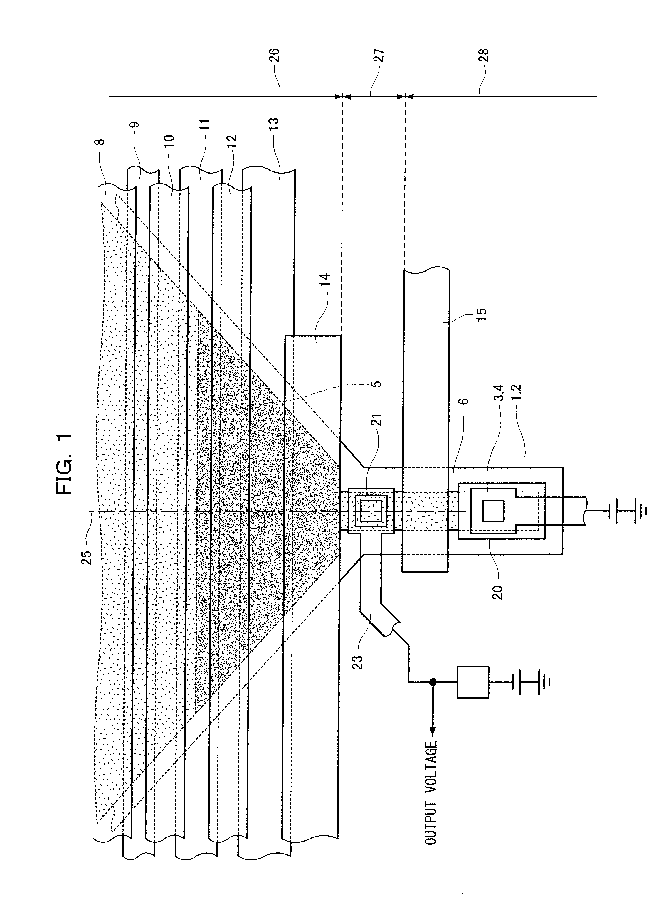
[0043]The structure of a solid state image sensor according to Embodiment 1 will be explained using FIG. 1, FIG. 2 and FIG. 3.

[0044]FIG. 1 shows a schematic plan view of a horizontal CCD (horizontal transfer) outlet of the solid state image sensor according to Embodiment 1 of the present invention. Furthermore, FIG. 2 is a schematic cross-sectional view of the horizontal CCD outlet of the solid state image sensor according to Embodiment 1 and shows a cross section including a gate electrode 13 which is the final stage of a horizontal CCD, a gate electrode 14 which is an offset gate, a region 27, a gate electrode 15 which is a reset gate, and an n-type region 20 which is a reset drain and viewed along a direction 25 parallel to a charge transfer direction. FIG. 3 shows a depletion potential at the time of charge transfer in the horizontal CCD channel of the solid state image sensor of Embodiment 1.

[0045]In FIG. 1, a region 26 including a gate electrode 8, a gate electrode 9, a gate e...

embodiment 2

[0071]The structure of a solid state image sensor according to Embodiment 2 will be explained using FIG. 4 and FIG. 5.

[0072]FIG. 4 shows a schematic plan view of a horizontal CCD outlet of the solid state image sensor according to Embodiment 2 of the present invention. FIG. 5 shows a schematic cross sectional view of the horizontal CCD outlet of the solid state image sensor according to Embodiment 2, which is a cross section in a direction 41 parallel to a charge transfer direction, including a gate electrode 51 which is a horizontal CCD final stage, a gate electrode 52 which is an offset gate, a region 43, a gate electrode 15 which is a reset gate and an n-type region 20 which is a reset drain.

[0073]First, this embodiment will be explained using FIG. 4 and FIG. 5. However, the same reference numerals as those in FIG. 1 and FIG. 2 indicate identical parts and explanations thereof will be omitted here.

[0074]In FIG. 4, a region 42 including a gate electrode 8, gate electrode 9, gate e...

embodiment 3

[0090]The structure of a solid state image sensor according to Embodiment 3 will be explained using FIG. 6, FIG. 7 and FIG. 8.

[0091]FIG. 6 shows a schematic plan view of a horizontal CCD outlet of the solid state image sensor according to Embodiment 3 of the present invention. FIG. 7 is a schematic cross-sectional view of the horizontal CCD outlet of the solid state image sensor according to Embodiment 3, which is a cross section in a direction 61 parallel to a charge transfer direction, including a gate electrode 73 which is a horizontal CCD final stage, a gate electrode 74 which is an offset gate, a region 63, a gate electrode 15 which is a reset gate and an n-type region 20 which is a reset drain. FIG. 8 shows a depletion potential in the horizontal CCD channel of the solid state image sensor according to Embodiment 3 at the time of charge transfer.

[0092]First, the configuration will be explained using FIG. 6 and FIG. 7. However, the same reference numerals as those in FIG. 1 and...


PUM


Abstract

Forming an impurity region 6 and an impurity region 5 having a lower concentration than the impurity region 6 in a lower layer region of a gate electrode close to the boundary with a signal electron-voltage conversion section of a horizontal CCD outlet makes it possible to smooth a potential distribution at the time of transfer, improve the transfer efficiency, increase the number of saturated electrons and reduce variations in the transfer efficiency and variations in saturation.

Description

FIELD OF THE INVENTION[0001]The present invention relates to a solid state image sensor made up of a horizontal transfer CCD section that receives signal electrons and transfers the signal electrons in a horizontal direction, an electron-voltage conversion section that converts the electrons transferred from the horizontal CCD section to a signal voltage and a reset drain section that discharges the electrons.BACKGROUND OF THE INVENTION[0002]With the miniaturization of cameras and increasing pixel counts, significant advances are being observed in cell miniaturization of downsizing pixel cells while increasing the number of electrons handled per unit area in CCD solid state image sensing elements used for HD video cameras and digital still cameras in classes over 10 million pixels for consumer and business applications. In addition, imaging with moving pictures is an indispensable function for these CCDs and this is required to be achieved concurrently with the speed-up of horizonta...

Claims


Application Information

Patent Timeline
IPC IPC(8): H01L27/148H01L21/339H01L29/762H04N5/335H04N5/341H04N5/369H04N5/372
CPCH01L27/14812
Inventor TACHIKAWA, KEISHI
Owner COLLABO INNOVATIONS INC
Why Eureka
Try Eureka