Display device
a display device and display technology, applied in static indicating devices, non-linear optics, instruments, etc., can solve the problems of increased delay of scan signal on scan signal line, difficult to avoid, and difficult to detect, so as to improve the display quality of active matrix display devices, improve the effect of variability in bias condition, and improve the effect of variation in bias condition
- Summary
- Abstract
- Description
- Claims
- Application Information
AI Technical Summary
Benefits of technology
Problems solved by technology
Method used
Image
Examples
embodiment 1
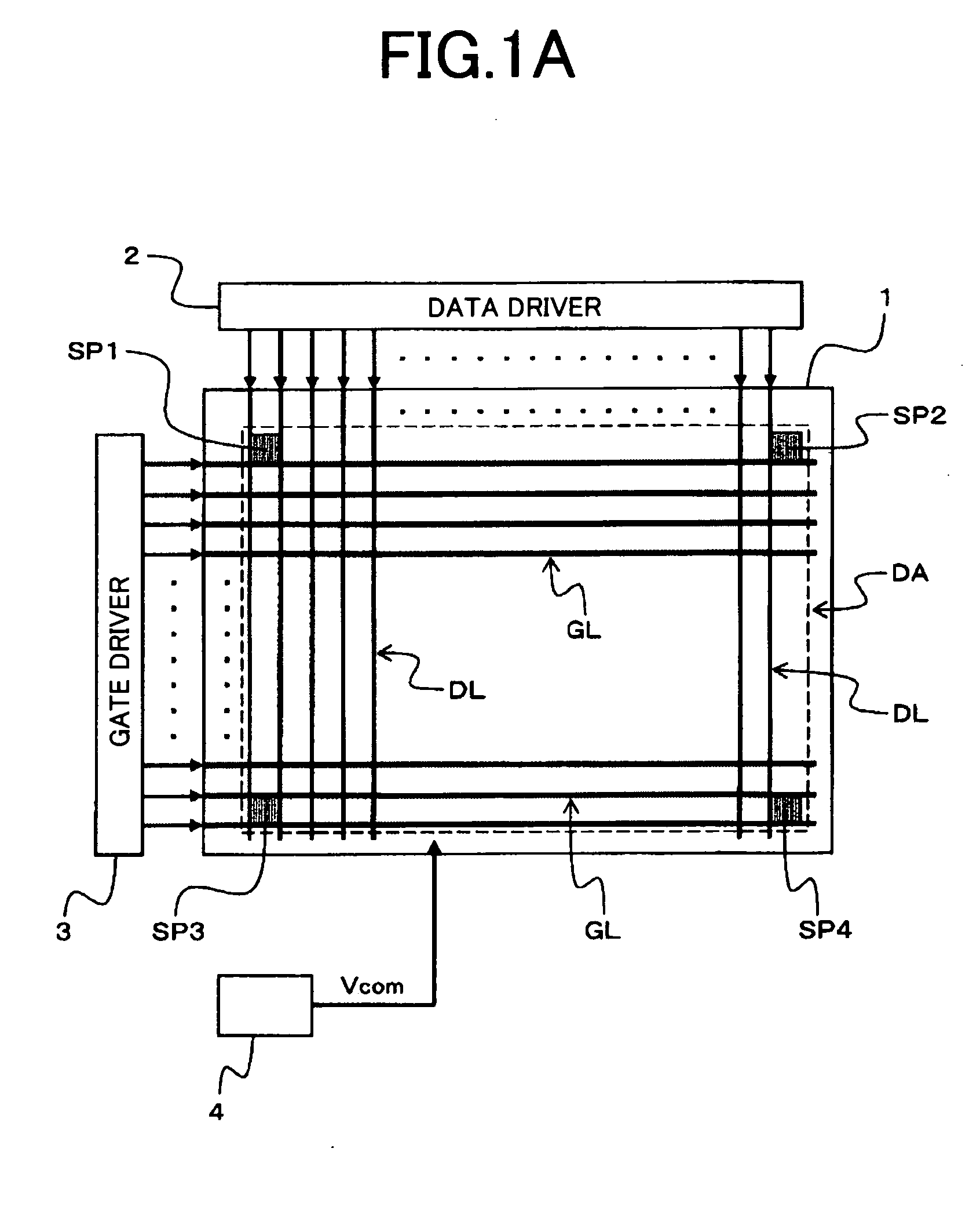
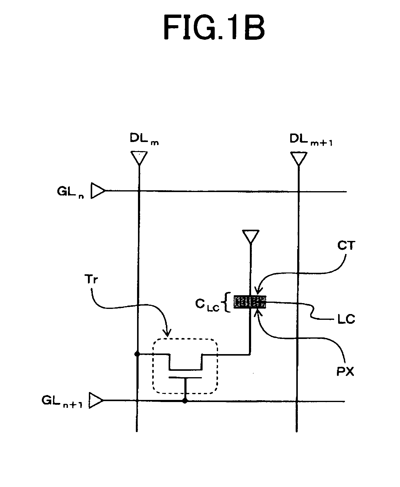
[0091]FIG. 4 is a model circuit diagram depicting an example of a simplified design of a liquid-crystal display panel according to Embodiment 1.
[0092]As shown in FIG. 4, in the liquid-crystal display panel according to Embodiment 1, the plurality of TFT elements Tr arranged in matrix form in the display area DA are distinguished using the notation Trn,m. The subscript “n” of Trn,m is any one of a number of integers 1, 2, . . . i, . . . N, and denotes the scan signal line GLn to which the gate is connected. The subscript I“m” of Trn,m is any one of a number of integers 1, 2, . . . j, . . . M, and denotes the picture signal lines DL, to which the drain is connected.
[0093]In FIG. 4, the triangular symbols at the left ends of the scan signal lines GL1, GLi−1, GLi, GLN−1, GLN denote signal input terminals for scan signals, while the triangular symbols at the upper ends of the picture signal lines DL1, DL2, DLj, DLj+1, DLM denote signal input terminals for picture signals.
[0094]Individual...
embodiment 2
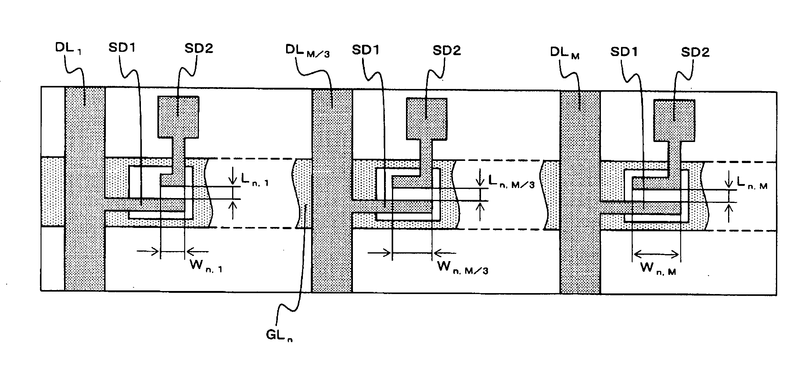
[0140]FIGS. 12A through 12D are model diagrams depicting an example of a simplified design of a TFT substrate according to Embodiment 2 of the present invention. FIG. 12A is a model plan view depicting an example of a design of an insulating substrate immediately following formation of a first insulating layer. FIG. 12B is a model sectional view of an example of a cross section taken along line D-D′ in FIG. 12A. FIG. 12C is a model plan view depicting an example of planar configuration of TFT elements of two pixels SP5, SP6 shown in FIG. 12A. FIG. 12D is a model graph depicting, for the liquid-crystal display panel according to Embodiment 2, an example of a relationship between the location of a single scan signal line and the thickness of the gate insulating film; an example of a relationship between the location of a single scan signal line and the pre-write voltage of pixels having TFT elements which are connected to a single common scan signal line; and an example of a method fo...
PUM
| Property | Measurement | Unit |
|---|---|---|
| area DA | aaaaa | aaaaa |
| length | aaaaa | aaaaa |
| width | aaaaa | aaaaa |
Abstract
Description
Claims
Application Information
 - R&D
- Intellectual Property
- Life Sciences
- Materials
- Tech Scout
- Unparalleled Data Quality
- Higher Quality Content
- 60% Fewer Hallucinations
Browse by: Latest US Patents, China's latest patents, Technical Efficacy Thesaurus, Application Domain, Technology Topic, Popular Technical Reports.
© 2025 PatSnap. All rights reserved.Legal|Privacy policy|Modern Slavery Act Transparency Statement|Sitemap|About US| Contact US: help@patsnap.com


