Mask pattern formation method, mask pattern formation apparatus, and lithography mask
a technology of mask pattern and mask pattern, which is applied in the direction of photomechanical treatment originals, program control, instruments, etc., can solve the problems of lithography verification taking a long time, the final finished pattern dimension on the wafer does not conform to the design pattern dimension, and it is difficult to faithfully form a pattern in each process
- Summary
- Abstract
- Description
- Claims
- Application Information
AI Technical Summary
Problems solved by technology
Method used
Image
Examples
first embodiment
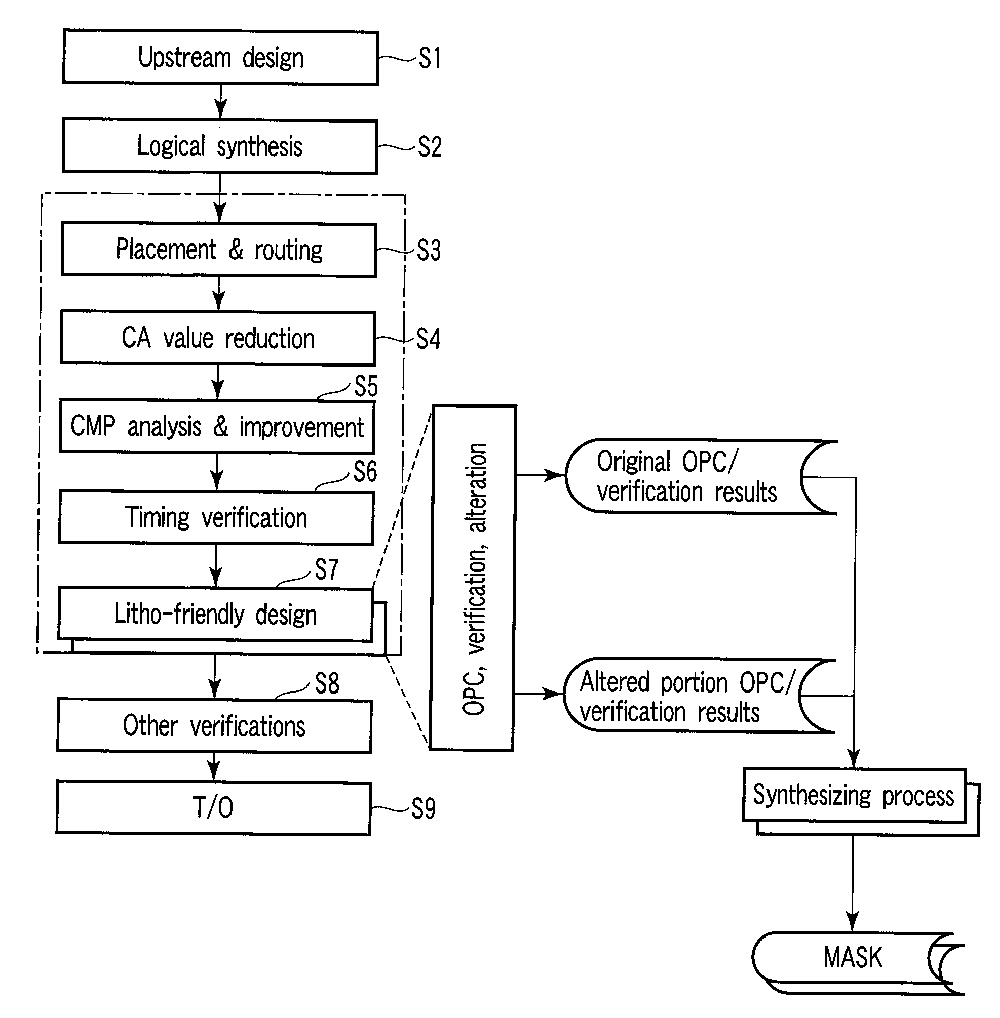
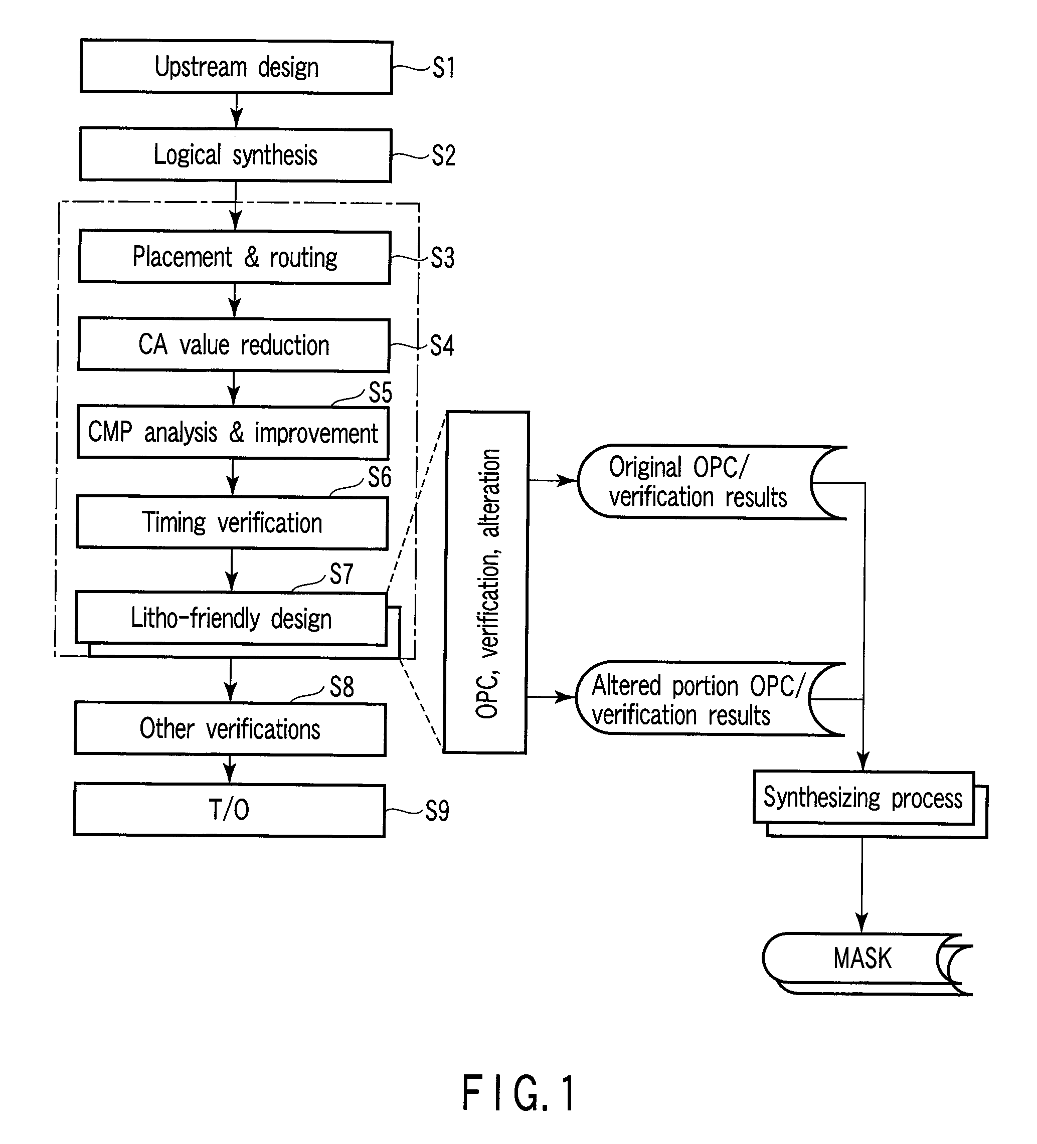
[0026]FIG. 1 is a flowchart for explaining the procedure of chip designing according to the first embodiment of the present invention.
[0027]First, as upstream design (step S1), the connection interval of blocks such as logic elements is described, and whether the input / output connections satisfy given criteria is checked by simulation. Then, logical synthesis that converts the blocks into logic blocks (AND, OR gates) is performed (step S2). The placement and routing of the logic blocks are determined on the basis of a cell library (step S3). That is, an efficient placement that reduces the necessary area is determined by taking the operation timing of each block into account.
[0028]Subsequently, the critical area is reduced, and the distances between interconnections are optimized (step S4). To planarize the surface of the substrate, processes such as a process of forming a dummy interconnection in a region where the distance between interconnections is long are performed (step S5). ...
second embodiment
[0044]FIGS. 4 and 5 are flowcharts for explaining the main part of the procedure of chip designing according to the second embodiment of the present invention, and illustrate exemplary examples of the procedure of litho-friendly design (step S7) shown in FIG. 1.
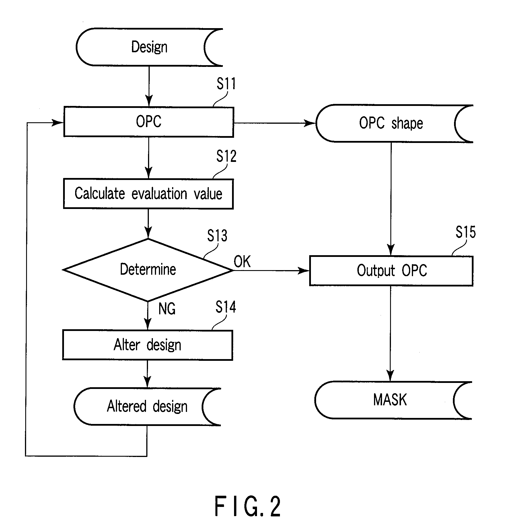
[0045]In the flowchart shown in FIG. 4, steps S11 to S14 are the same as in FIG. 2.
[0046]This embodiment differs from the first embodiment (FIG. 2) in that if it is determined in step S13 that the evaluation value calculated in step S12 satisfies the predetermined value, the evaluation value finally obtained in step S12 is extracted and output (step S25). It is also possible to simultaneously output the process optical proximity correction result obtained in step S11. The output result is recorded as manufacturing control data.
[0047]In the flowchart shown in FIG. 5, steps S11 to S16 are the same as in FIG. 3.
[0048]This embodiment differs from the first embodiment (FIG. 3) explained previously in that if it is determined in st...
third embodiment
[0051]FIG. 6 is a flowchart for explaining the main part of the procedure of chip designing according to the third embodiment of the present invention, and shows an exemplary example of the processing using litho-friendly design (step S7) shown in FIG. 1.
[0052]The basic flow from steps S11 to S15 is the same as in FIG. 2.
[0053]This embodiment is characterized in that in step S12, design rule verification, circuit connection verification, timing verification, voltage drop verification, coverage verification, critical area verification, the calculation of an evaluation value for a finished planar shape of the resist pattern on a wafer, and the like are performed on the design layout input in step S11, on the basis of various kinds of information stored in a storage unit S30. In step S12, it is not always necessary to perform all the verifications and calculations, and it is also possible to selectively perform one or more of these verifications and calculations.
[0054]In the first embo...
PUM
| Property | Measurement | Unit |
|---|---|---|
| size | aaaaa | aaaaa |
| optical radius | aaaaa | aaaaa |
| radius | aaaaa | aaaaa |
Abstract
Description
Claims
Application Information
 - R&D
- Intellectual Property
- Life Sciences
- Materials
- Tech Scout
- Unparalleled Data Quality
- Higher Quality Content
- 60% Fewer Hallucinations
Browse by: Latest US Patents, China's latest patents, Technical Efficacy Thesaurus, Application Domain, Technology Topic, Popular Technical Reports.
© 2025 PatSnap. All rights reserved.Legal|Privacy policy|Modern Slavery Act Transparency Statement|Sitemap|About US| Contact US: help@patsnap.com


