
Nonvolatile memory control device, nonvolatile memory control method, and storage device

a control device and non-volatile technology, applied in the direction of memory adressing/allocation/relocation, instruments, computing, etc., can solve the problems of increasing the occurrence of data errors, complex physical block management, and time-consuming

Inactive Publication Date: 2008-12-25
KK TOSHIBA
View PDF19 Cites 30 Cited by
  • Summary
  • Abstract
  • Description
  • Claims
  • Application Information

AI Technical Summary

Benefits of technology

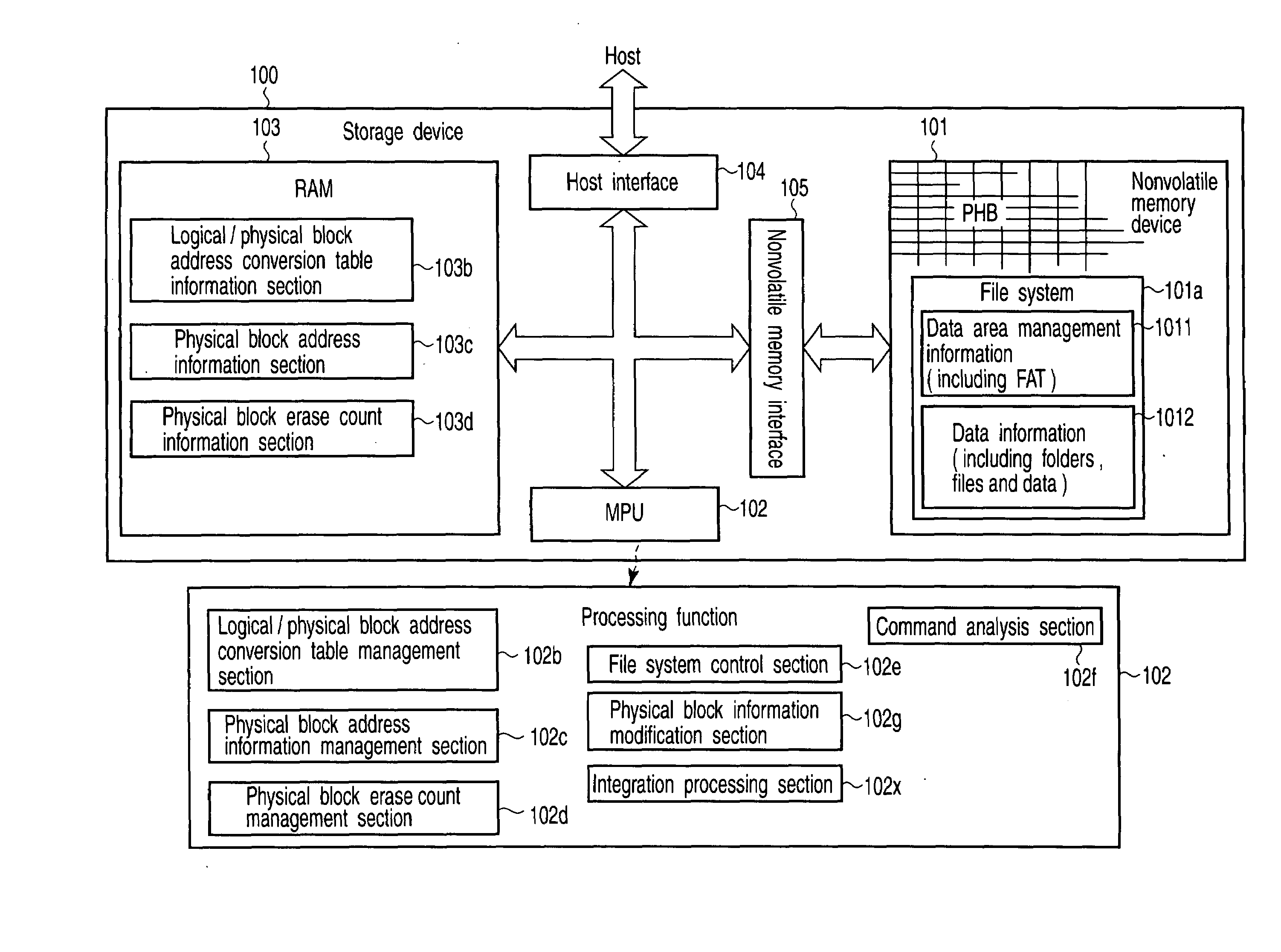
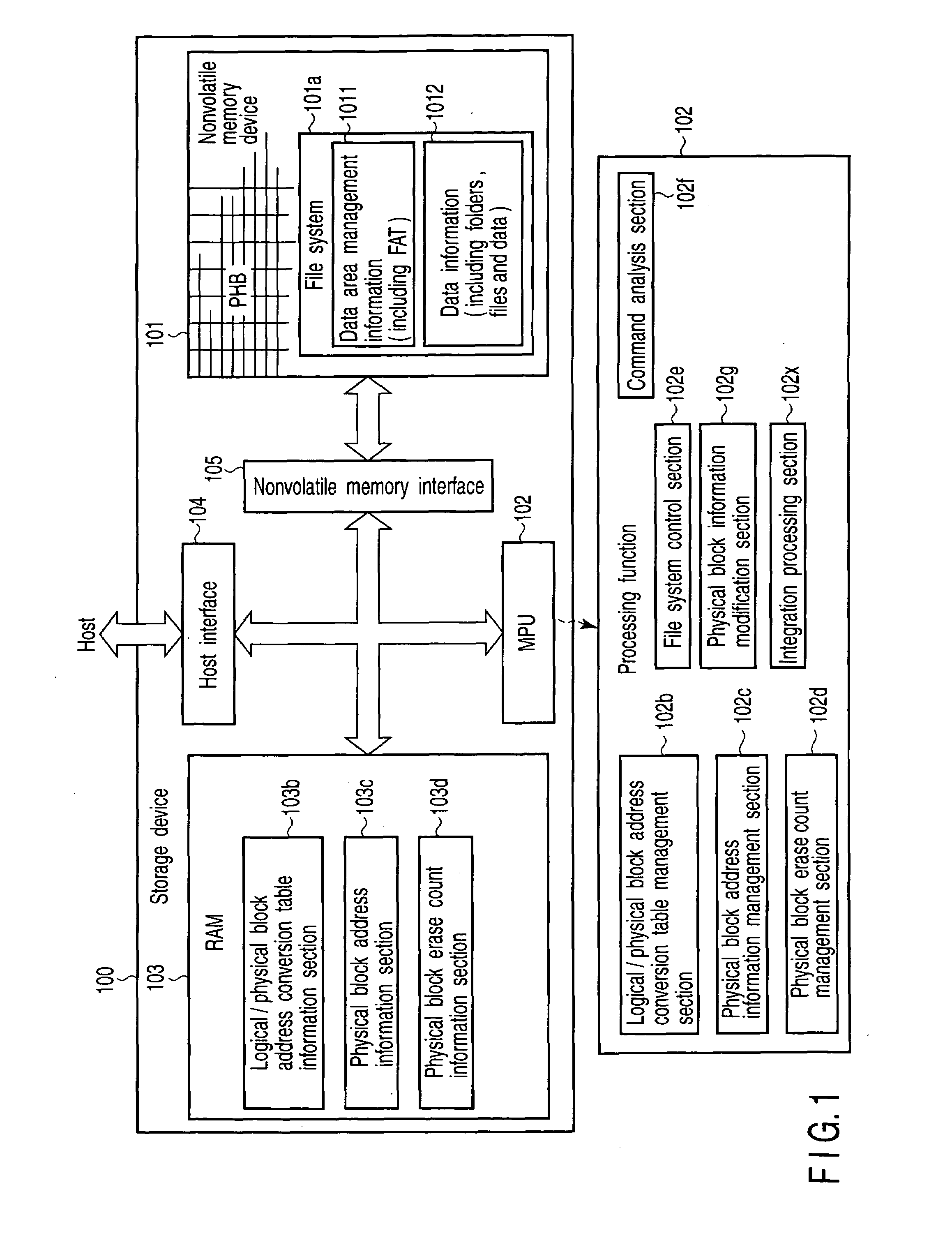
The present invention relates to a nonvolatile memory control device, method, and storage device that can manage the number of times a physical block is erased to prevent data errors and improve performance. The invention uses information of a file system, such as the FAT, to identify unused logical blocks and release the association between them. This allows for the management of a large number of arbitrarily available physical blocks. The invention also includes a file system controller, a logical / physical block address conversion table management section, and a physical block address information management section to facilitate the averaging processing of the number of times of physical block erase operation. The technical effect of the invention is to increase the number of arbitrarily available physical blocks in a nonvolatile memory device and improve the performance of the device by managing the number of times a physical block is erased.

Problems solved by technology

When the number of times of the erase or write operation is increased, device degradation occurs to result in an increase in occurrence of data errors.
Therefore, management of the physical block and averaging processing of the number of times of the erase operation are complicated and time-consuming.

Method used


Image

  • Nonvolatile memory control device, nonvolatile memory control method, and storage device
  • Nonvolatile memory control device, nonvolatile memory control method, and storage device
  • Nonvolatile memory control device, nonvolatile memory control method, and storage device

Examples


Embodiment Construction

[0023]Various embodiments according to the invention will be described hereinafter with reference to the accompanying drawings.

[0024]An object of the embodiments of the present invention is to provide a nonvolatile memory control device, a nonvolatile memory control method, and a storage device capable of increasing the number of arbitrarily available physical blocks in a nonvolatile memory device by using information of a file system, especially, information of a file allocation table and thus capable of facilitating and speeding up averaging processing (alternation between physical blocks) of the number of times of the physical block erase operation.

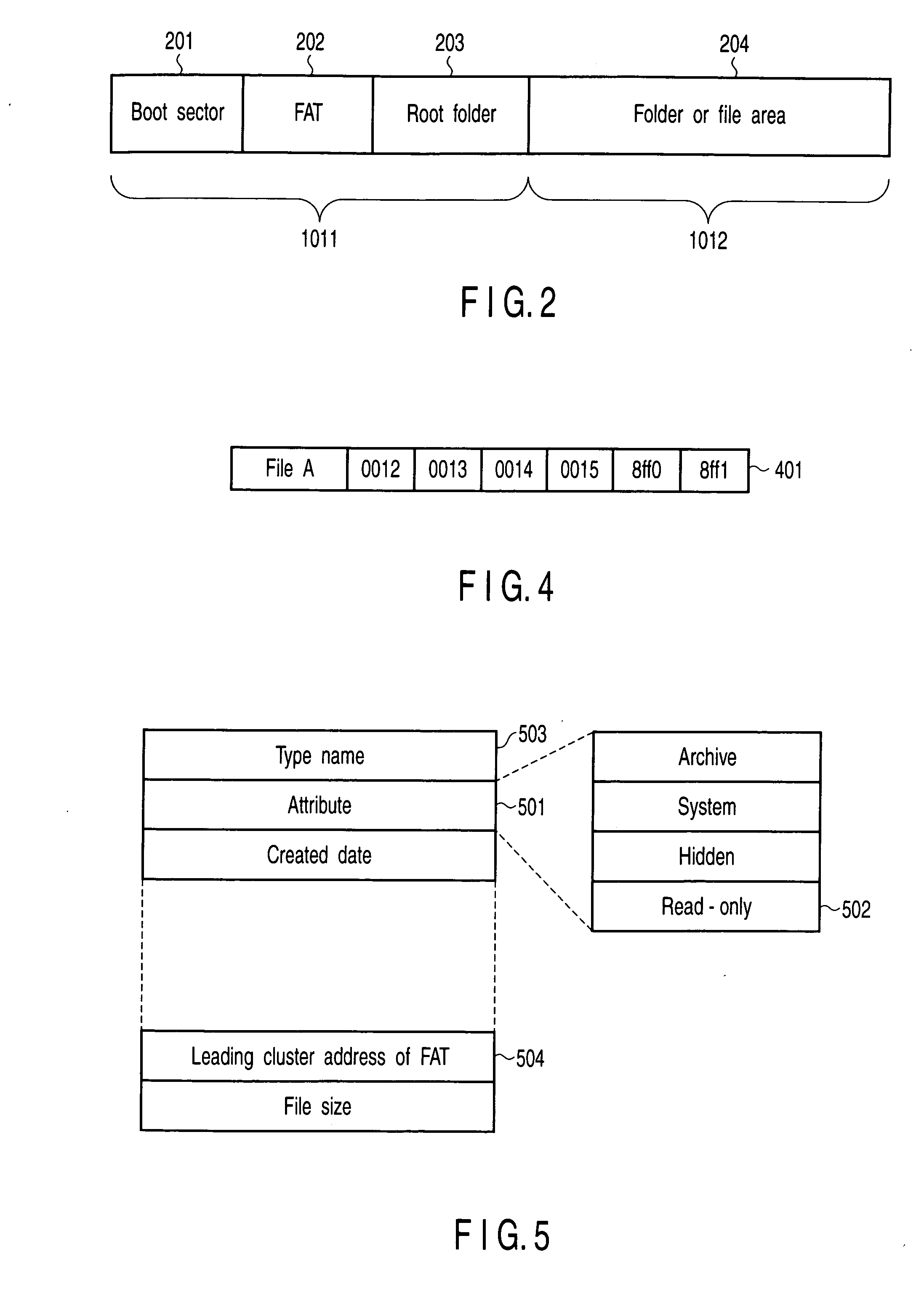
[0025]According to one aspect of the present invention, there is provided a nonvolatile memory control device comprising: a file system controller which analyzes a file allocation table (FAT) in a file system of a nonvolatile memory device to identify an unused logical block; a logical / physical block address conversion table management...


PUM


Abstract

According to an embodiment of the present invention is to increase the number of arbitrarily available physical blocks in a nonvolatile memory device. The device comprises a file system control section which analyzes a file allocation table (FAT) to identify an unused logical block, a logical / physical block address conversion table management section which uses a table of a logical / physical block address conversion table information section to obtain a first physical block corresponding to the unused logical block and releases the association between the first physical block and the unused logical block, and a physical block address information management section which registers the first physical block in a physical block address information section as an arbitrarily available second physical block.

Description

CROSS-REFERENCE TO RELATED APPLICATIONS[0001]This application is based upon and claims the benefit of priority from Japanese Patent Application No. 2007-165368, filed Jun. 22, 2007, the entire contents of which are incorporated herein by reference.BACKGROUND[0002]1. Field[0003]One embodiment of the invention relates to a nonvolatile memory control device, a nonvolatile memory control method, and a storage device.[0004]Particularly, the embodiments of the present invention are characterized in a nonvolatile memory management method that uses information of a file system to manage a logical block address-physical block address conversion table and an arbitrarily available physical block.[0005]2. Description of the Related Art[0006]A NAND-type flash memory is known as a data rewritable nonvolatile memory. The data erase unit of the nonvolatile memory is one block (e.g., 128 kbytes). On the other hand, the data read and write units of the nonvolatile memory are set to 2 kbytes. When the...

Claims


Application Information

Patent Timeline
Patent Type & Authority Applications(United States)
IPC IPC(8): G06F12/02G06F12/00G06F12/10
CPCG06F3/0616G06F3/064G06F3/0679G06F12/0246G06F2212/1036G06F2212/7211
Inventor KINOSHITA, TADAAKI
Owner KK TOSHIBA
Learn More