Eureka AIR delivers breakthrough ideas for toughest innovation challenges, trusted by R&D personnel around the world.

Protecting Trade Secrets During the Design and Configuration of an Integrated Circuit Semiconductor Design

Active Publication Date: 2008-09-11
ARM FINANCE OVERSEAS LTD
View PDF11 Cites 18 Cited by
  • Summary
  • Abstract
  • Description
  • Claims
  • Application Information

AI Technical Summary

Benefits of technology

[0010]In a third aspect of the invention, an apparatus for generating, simulating, and/or synthesizing a SoC design using the aforementioned m

Problems solved by technology

Complex systems have always been hard to build and debug.
However, the integrated circuit industry has developed rapidly over the last several years from producing VLSI devices that integrate a processor, memory and a few peripheral components onto a single chip to today's complex, high-performance systems on chip (SoC) that incorporate hundreds of intellectual property (IP) blocks.
Because the economics of integrated circuit manufacture do not allow debugging by trial and error; the design must be ‘right first time’.
As a result, SoC designers must minimize the risk of design error because any design iteration will be expensive in both mask charges and time to market.
While well suited for simpler devices and single components, the aforementioned synthesis process suffers several limitations, especially when applied to the design of complex SoCs.

Method used


Image

  • Protecting Trade Secrets During the Design and Configuration of an Integrated Circuit Semiconductor Design
  • Protecting Trade Secrets During the Design and Configuration of an Integrated Circuit Semiconductor Design
  • Protecting Trade Secrets During the Design and Configuration of an Integrated Circuit Semiconductor Design

Examples


Embodiment Construction

[0026]Reference is now made to the drawings wherein like numerals refer to like parts throughout.

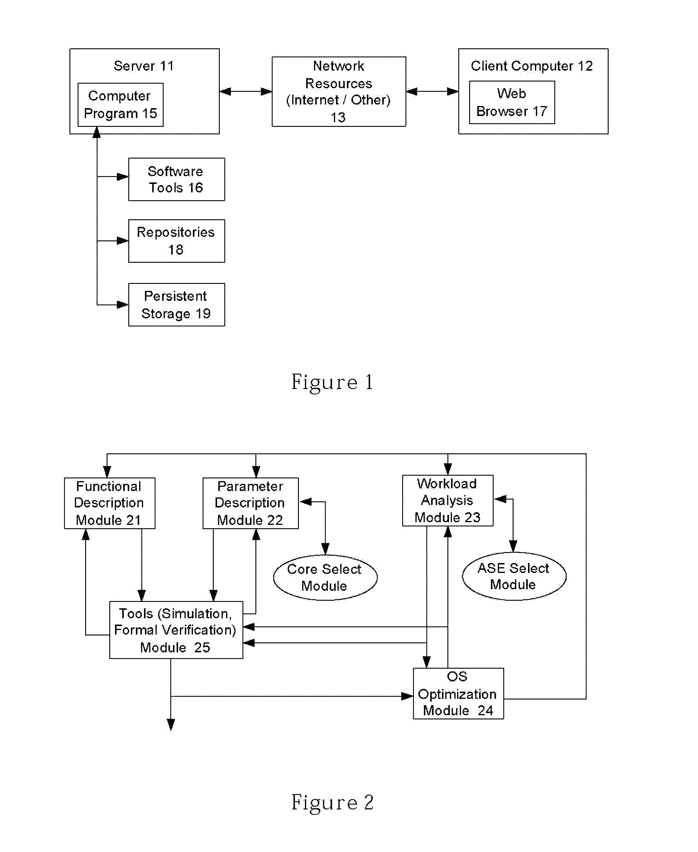
[0027]As illustrated in FIG. 1, the present invention for managing the design and configuration of a system on a chip (SoC) or other silicon design takes, in one embodiment, the form of a server 11 coupled to at least one client computer 12 by a network 13 such as the Internet. The method provides for the automated description of hardware components, such as a processor core, specialized processors, buses and controllers, and software components, such as application and operating software, as well as the integration of the hardware and software components.

[0028]A silicon-on-chip (SoC) designer accesses server-resident computer program 15 and software tools 16 using a web browser 17 installed on client computer 12. It will be appreciated, that server 11 may be one server in a data center environment or the functions described herein may be distributed among a plurality of servers to load ...


PUM


Abstract

A system and method for facilitating the design process of an integrated circuits (IC) is described. The system and method utilizes a plurality of repositories, rules engines and design and verification tools to analyze the workload and automatically produce a hardened GDSII description or other representation of the IC. Synthesizable RTL is securely maintained on a server in a data center while providing designers graphical access to customizable IP block by way of a network portal.

Description

FIELD OF THE INVENTION[0001]The invention relates generally to the field of integrated circuits (IC) design. More specifically the present invention relates to a system and method that protects trade secrets relating to the design process of an IC comprising third party intellectual property (IP).DESCRIPTION OF RELATED TECHNOLOGY[0002]Complex systems have always been hard to build and debug. However, the integrated circuit industry has developed rapidly over the last several years from producing VLSI devices that integrate a processor, memory and a few peripheral components onto a single chip to today's complex, high-performance systems on chip (SoC) that incorporate hundreds of intellectual property (IP) blocks. Because the economics of integrated circuit manufacture do not allow debugging by trial and error; the design must be ‘right first time’. As a result, SoC designers must minimize the risk of design error because any design iteration will be expensive in both mask charges an...

Claims


Application Information

Patent Timeline
IPC IPC(8): G06F17/50
CPCG06F17/5045G06F30/30
Inventor BANERJEE, SOUMYA
Owner ARM FINANCE OVERSEAS LTD
Why Eureka
Eureka Blog
Learn More