Plasma display panel and method for driving same
a technology of plasma display panel and display panel, which is applied in the direction of static indicating devices, instruments, gas-filled discharge tubes, etc., can solve the problems of visible light emission, reduce the light emission caused by reset discharge and observed on the panel screen, and prevent the reduction of dark contrast. , the effect of improving the dark contrast of the pdp
- Summary
- Abstract
- Description
- Claims
- Application Information
AI Technical Summary
Benefits of technology
Problems solved by technology
Method used
Image
Examples
first embodiment
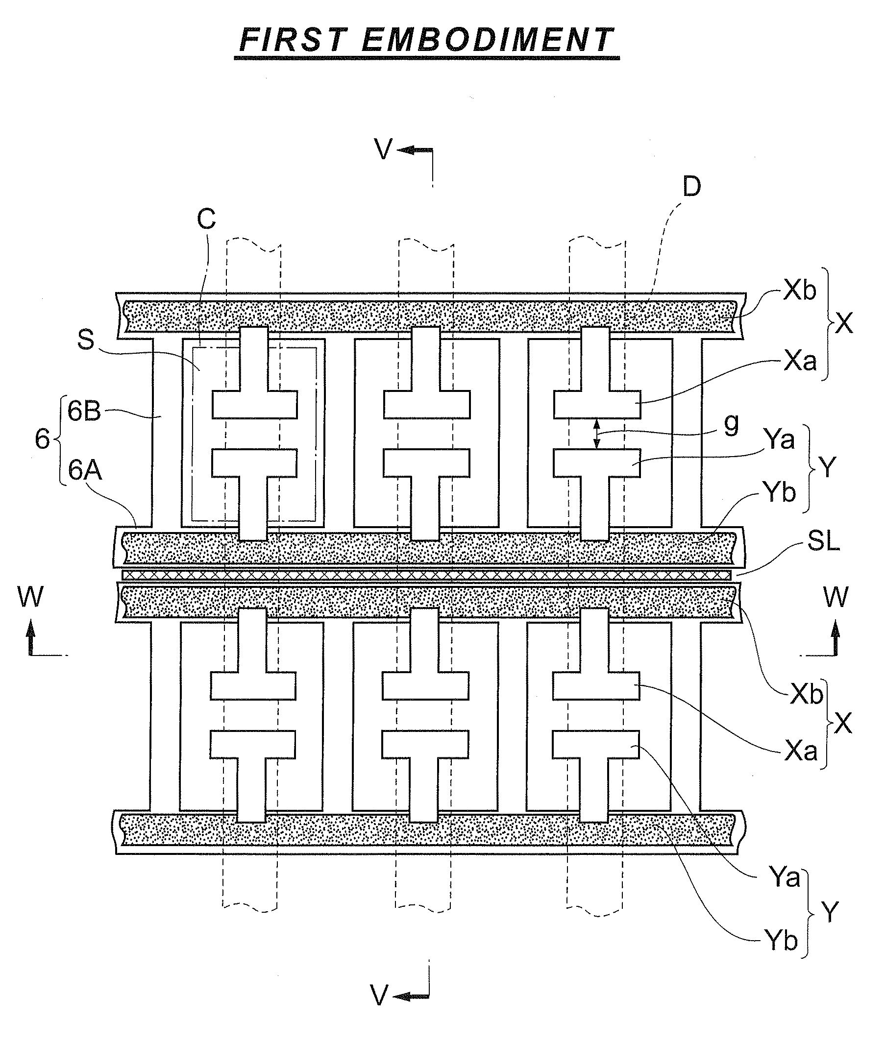
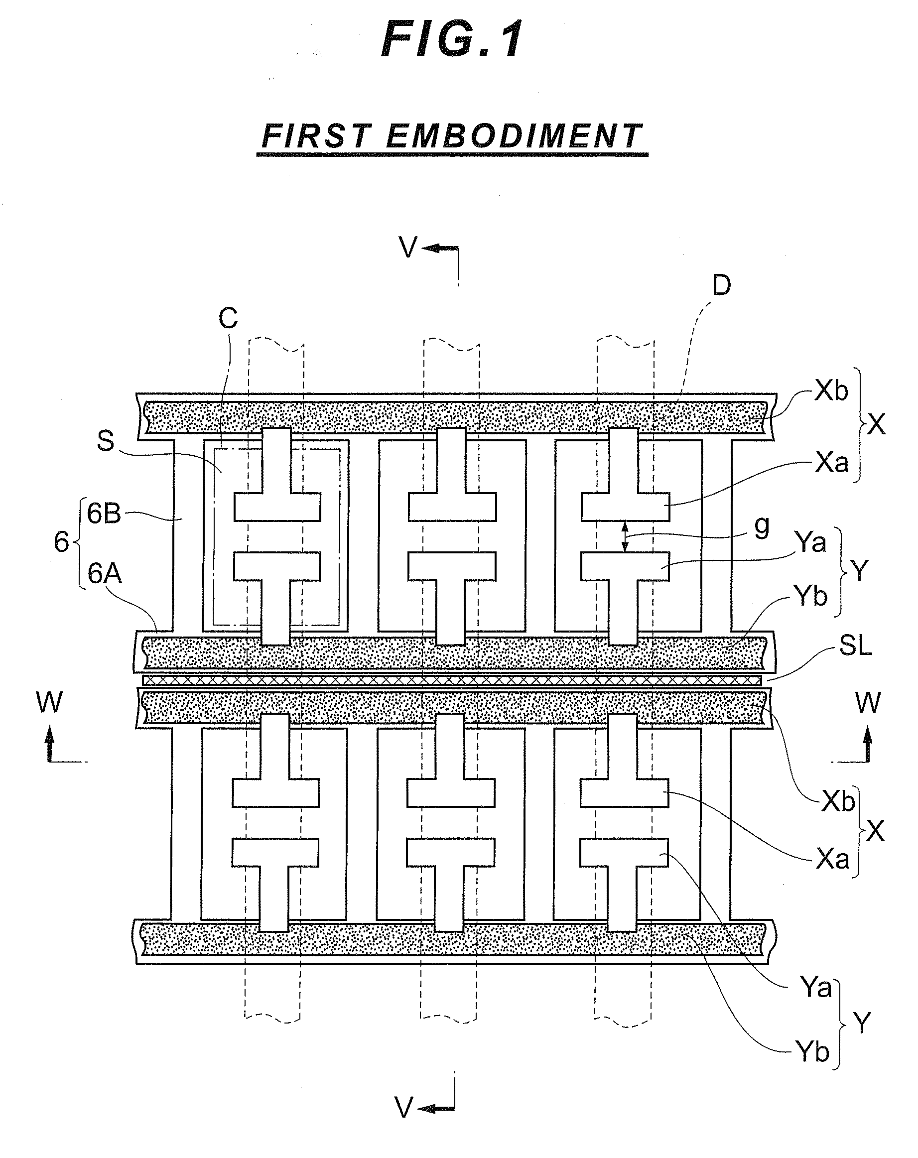
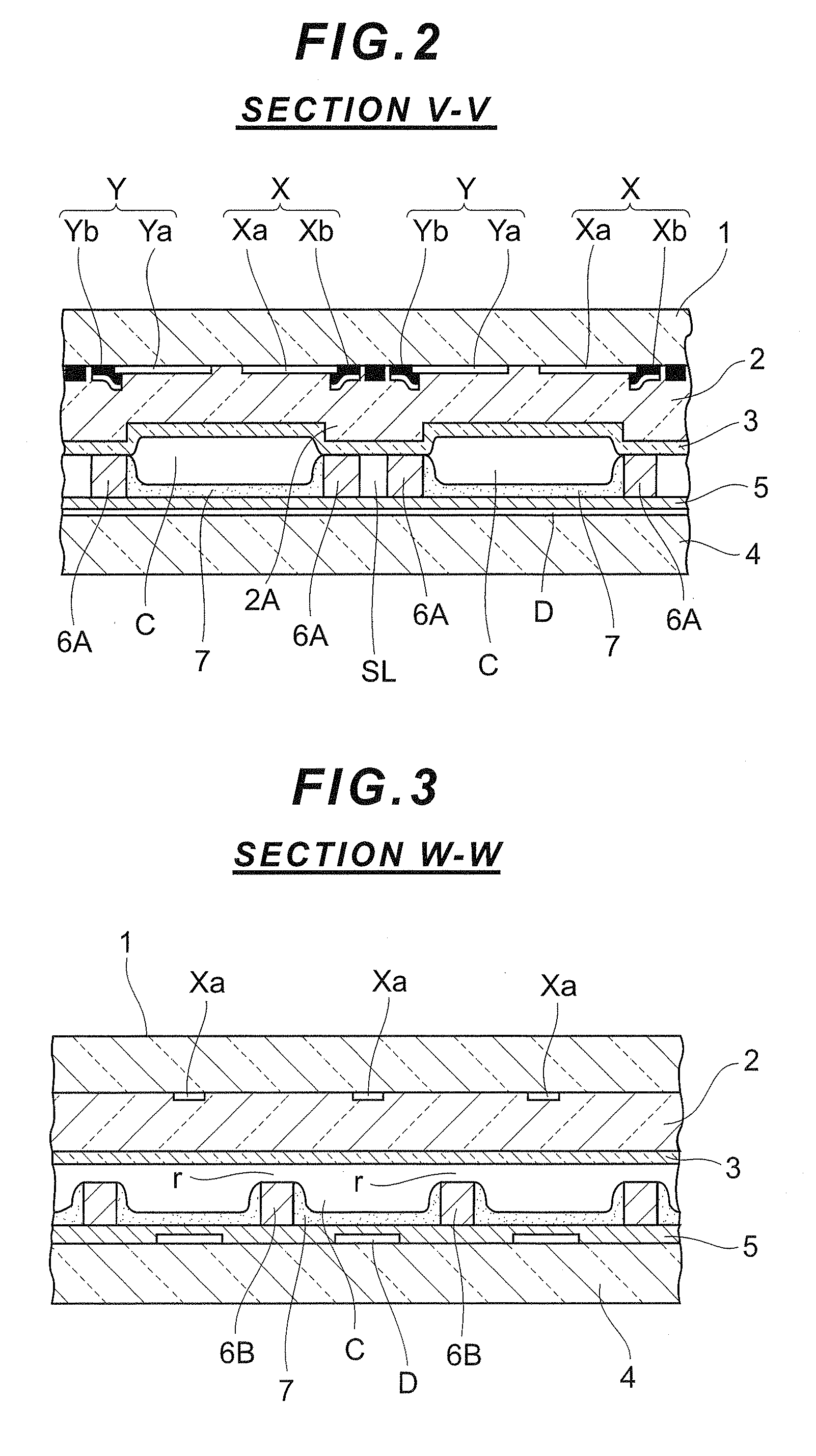
[0069]FIGS. 1 to 3 illustrate a first embodiment of the PDP according to the present invention. FIG. 1 is a schematic front view of the PDP in the first embodiment. FIG. 2 is a sectional view taken along the V-V line in FIG. 1. FIG. 3 is a sectional view taken along the W-W line in FIG. 1.
[0070]The PDP in FIGS. 1 to 3 has a plurality of row electrode pairs (X, Y) arranged in parallel on the rear-facing face (the face facing toward the rear of the PDP) of a front glass substrate 1 serving as the display surface so as to extend in the row direction of the front glass substrate 1 (the right-left direction in FIG. 1).
[0071]A row electrode X is composed of T-shaped transparent electrodes Xa formed of a transparent conductive film made of ITO or the like, and a bus electrode Xb formed of a metal film extending in the row direction of the front glass substrate 1 and connected to the narrow proximal ends of the transparent electrodes Xa.
[0072]Likewise, a row electrode Y is composed of T-sha...
second embodiment
[0175]FIG. 25 is a sectional view illustrating a second embodiment of the PDP according to the present invention.
[0176]The phosphor layer of the PDP described in the first embodiment is formed of a mixture of the phosphor material and the MgO crystal which is the secondary electron emission material. In the PDP of this second embodiment, a red phosphor layer 17(R), a green phosphor layer 17(G) and a blue phosphor layer 17(B) are respectively composed of a red phosphor material layer 17(R)A, a green phosphor material layer 17(G)A and a blue phosphor material layer 17(B)A which are respectively formed of red, green and blue phosphor materials, and MgO crystal layers 17(R)B, 17(G) B, 17(B)B which are respectively formed of MgO crystal which is the secondary electron emission material and are stacked on the respective red, green and blue phosphor material layers 17(R)A, 17(G)A, 17(B)A. The MgO crystal layers 17(R)B, 17(G)B, 17(B)B are exposed to the inside of the corresponding discharge...
third embodiment
[0186]Next, a third embodiment of the PDP according to the present invention will be described.
[0187]In the example of each of the first and second embodiment, the green phosphor layer includes a larger amount of the secondary electron emission material than those in the red phosphor layer and the blue phosphor layer in order to produce a clearer white display. The PDP in the third embodiment has the structure of the red, green and blue phosphor layers for improving the white display, and additionally, the structure for preventing the black level luminance from decreasing because of the phosphor layer mixed with the secondary electron emission material.
[0188]The third embodiment is applicable to both the PDP of the first embodiment in FIG. 4 and the PDP of the second embodiment in FIG. 25, but the following description is the case when the third embodiment is applied to the PDP in FIG. 4.
[0189]In FIG. 4, the MgO crystal 7B as the secondary electron emission material is mixed in each...
PUM
 Abstract
Description
Claims
Application Information
 - R&D
- Intellectual Property
- Life Sciences
- Materials
- Tech Scout
- Unparalleled Data Quality
- Higher Quality Content
- 60% Fewer Hallucinations
Browse by: Latest US Patents, China's latest patents, Technical Efficacy Thesaurus, Application Domain, Technology Topic, Popular Technical Reports.
© 2025 PatSnap. All rights reserved.Legal|Privacy policy|Modern Slavery Act Transparency Statement|Sitemap|About US| Contact US: help@patsnap.com


