
Component Based on Organic Light-Emitting Diodes and Method For Producing the Same

a technology of organic light-emitting diodes and components, which is applied in the manufacture of electrode systems, electric discharge tubes/lamps, discharge tubes luminescnet screens, etc., can solve the problems of reducing the waveguide properties of individual layers within the display, reducing the efficiency of the display, and not allowing the current attainment of fill factors

Inactive Publication Date: 2008-07-10
NOVALED GMBH
View PDF5 Cites 44 Cited by
  • Summary
  • Abstract
  • Description
  • Claims
  • Application Information

AI Technical Summary

Problems solved by technology

In addition to these, there are also flat type display technologies such as plasma displays, vacuum fluorescence or field emission displays which are technically very sophisticated and cost-intensive.
This restriction is mainly caused by the masking of the organic layers because, with a full-colour display without filter or conversion layers, it is necessary to process red, green and blue sub-pixels next to each other.
The shadow masks used here for this purpose, and the error tolerances related to such, do not allow at present the attainment of fill factors that would be possible based on the manufacturing accuracy of the backplane.
The reduction of the waveguide properties of individual layers within the display by the stated approaches, however, does not improve the fill factor of a pixelled structural element.
However, the image information of the display gets partially lost because over-radiation and feedover occur between the individual pixels.
Care must be exercised in this case that the metal is only briefly sputtered on in order to avoid the formation of a continuous metal film instead of individual metal clusters, so that an isolation through the layer is no longer ensured.

Method used


Image

  • Component Based on Organic Light-Emitting Diodes and Method For Producing the Same
  • Component Based on Organic Light-Emitting Diodes and Method For Producing the Same
  • Component Based on Organic Light-Emitting Diodes and Method For Producing the Same

Examples


first embodiment

[0056]FIG. 3a an arranged display according to the invention with top emission;

[0057]FIG. 3b for the display shown in FIG. 3a, the arrangement of optically effective heterogeneities in the isolation layer with reference to the pixel structuring;

second embodiment

[0058]FIG. 4a an arranged display according to the invention with bottom emission;

[0059]FIG. 4b for the display shown in FIG. 4a, the arrangement of optically effective heterogeneities in the isolation layer with reference to the pixel structuring;

third embodiment

[0060]FIG. 5 a display according to the invention with top emission in a principle sketch with surface structured isolation layer;


PUM


Abstract

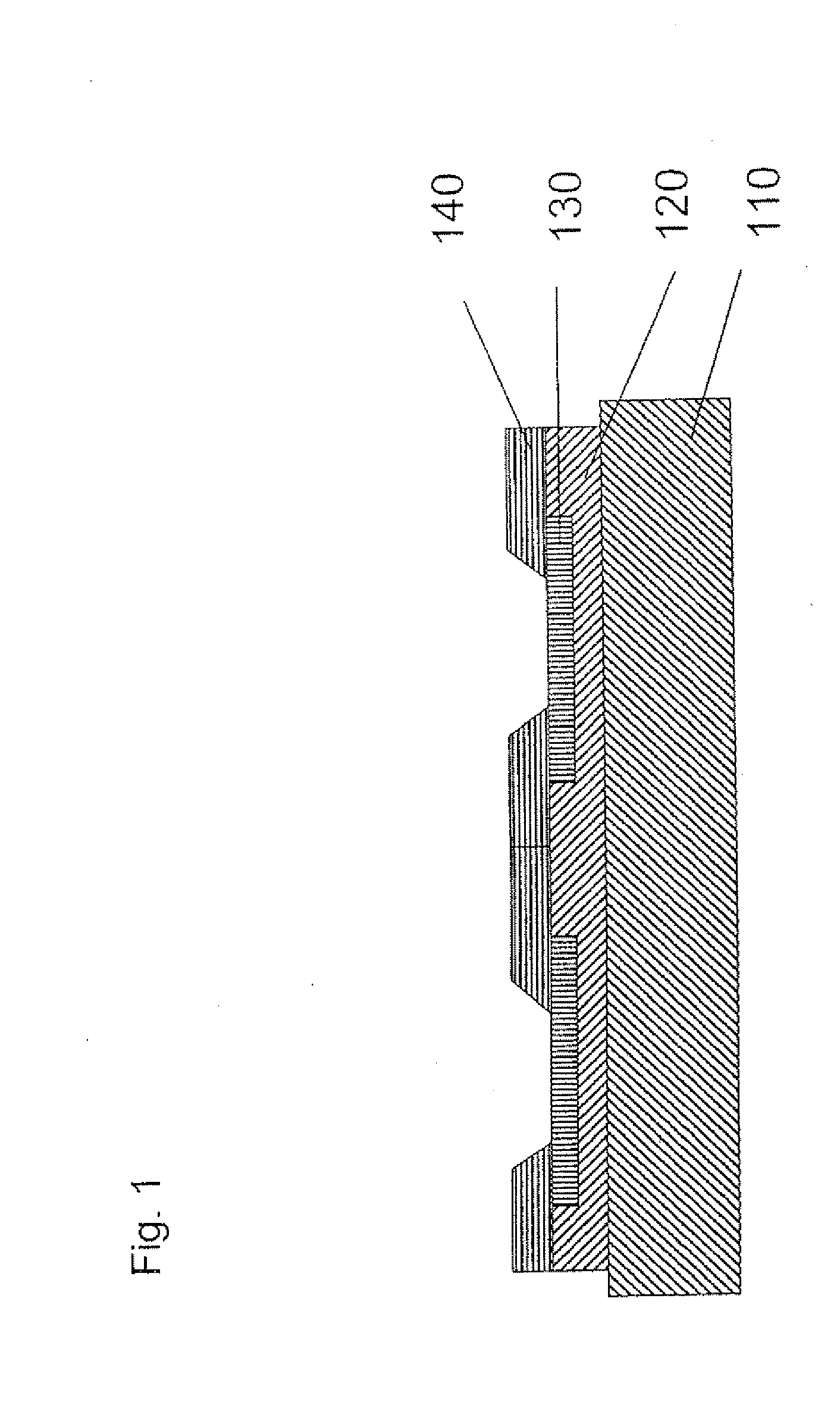
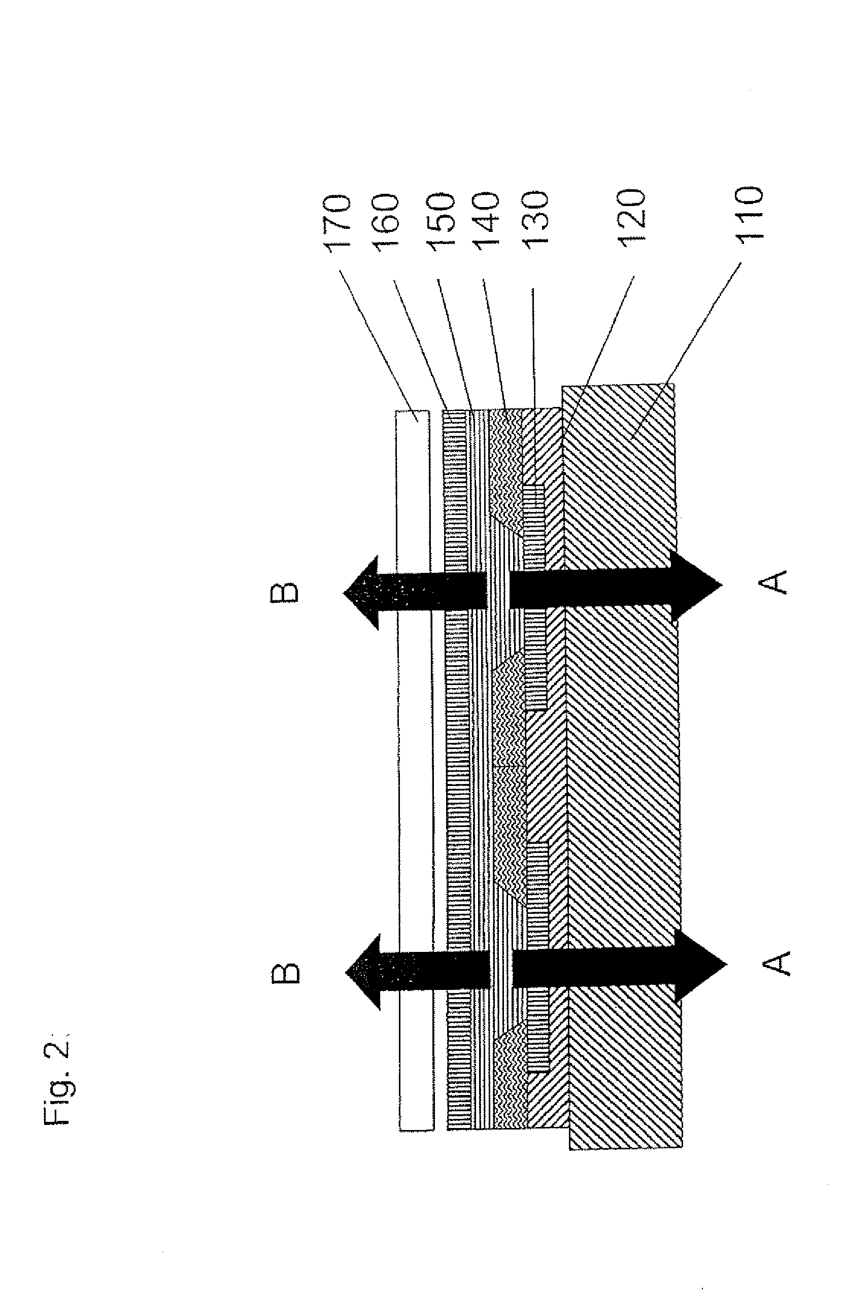
In order to improve the fill factor as well as the efficiency for a structural element on the basis of an organic light-emitting diode facility, a display is proposed comprising a substrate, a first electrode (130) nearest to the substrate, a second electrode (160) away from the substrate and at least one light-emitting organic layer (150) arranged between both electrodes. The light emitted in the active zone transmits through one of the two electrodes whereby the first electrode is pixel-structured and an isolation layer (150) is arranged between neighbouring pixels. The display according to the invention is characterized in that the isolation layer (150) is optically coupled with the light-emitting layer (150), and has optically effective light-scattering and fill factor increasing heterogeneities (180, 190), whereby the isolation layer is micro-structured to match the pixel structure of the first electrode and is processed onto this.In addition, the invention concerns also a method for the manufacture of such a display.

Description

[0001]The invention concerns a display on the basis of an organic light-emitting diode facility as well as a method for its manufacture.BACKGROUND OF THE INVENTION[0002]In recent years there has been an upsurge in the demand for increasingly smaller, space-saving, light and inexpensive display modules and displays for quick and adequate visualisation of data and information. The principle of the cathode steel tube or the liquid crystal display (LCD) is adopted for most of the display elements used at present. In addition to these, there are also flat type display technologies such as plasma displays, vacuum fluorescence or field emission displays which are technically very sophisticated and cost-intensive. With displays on the basis of organic light-emitting diodes (OLEDs), competition for the established technologies has emerged in recent years and this competition is to be taken seriously. The essential advantages of a display facility on the basis of OLEDs are stated as being the...

Claims


Application Information

Patent Timeline
IPC IPC(8): H01L27/32H01J9/02
CPCH01L51/5268H01L27/3246H10K59/122H10K59/877H10K50/854
Inventor HOFMANN, MICHAELBIRNSTOCK, JANVEHSE, MARTIN
Owner NOVALED GMBH
Learn More