Image display apparatus, manufacturing method of image display apparatus, and functional film

Inactive Publication Date: 2008-07-03
CANON KK +1
View PDF20 Cites 3 Cited by
  • Summary
  • Abstract
  • Description
  • Claims
  • Application Information

AI Technical Summary

Benefits of technology

[0023]An object of the present invention is to provide an image display apparatus that is provided with an conductive layer for satisfying electric functions such as (1) to prevent the electric charge of the image display area (2) while preventing increase of the electric charge amount of the metal back in a functional film to be mounted on an image display area of a face plate.
[0037]According to the present invention, even if electric discharge is generated inside the image display apparatus, it is possible to keep a current limiting effect of the anode electrode and to prevent increase of a potential of the image display area of the image display apparatus.

Problems solved by technology

As a result, the electron-emitting device 10002 is destroyed and the drive circuit to be connected to the row wiring 10003 and the column wiring 10004 is destroyed, and this may cause a serious deterioration of an image quality.
However, if charging inhibition processing is provided on the surface of the face plate by grounding the conductive layer as described above while giving the current limiting function to the anode electrode, a serious deficit of a pixel may be caused.

Method used


Image

  • Image display apparatus, manufacturing method of image display apparatus, and functional film
  • Image display apparatus, manufacturing method of image display apparatus, and functional film
  • Image display apparatus, manufacturing method of image display apparatus, and functional film

Examples


first embodiment

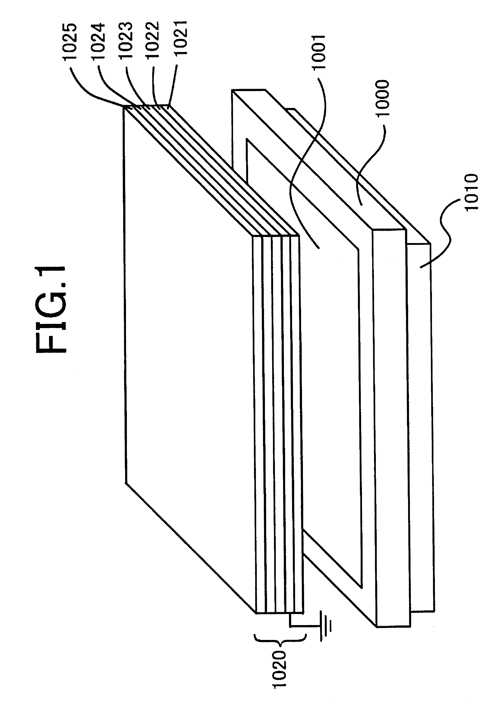
[0051]At first, an image display apparatus according to the first embodiment of the present invention will be described below. In FIG. 1, a typical view of an image display apparatus according to the first embodiment of the present invention is shown.

[0052]The image display apparatus according to the present embodiment is configured by an image display apparatus main body (a display panel) 1000, a drive circuit 1010, and a functional film 1020. In FIG. 1, the image display apparatus main body 1000 is separated from the functional film 1020; however, in the real constitution, the functional film 1020 is allowed to contact the image display area 1001 of the image display apparatus main body 1000. In addition, although the drive circuit 1010 is provided on the rear face of the image display apparatus main body 1000 in FIG. 1, the arrangement position of the drive circuit is not limited to such an arrangement position.

[0053]According to the present embodiment, an example of using the su...

second embodiment

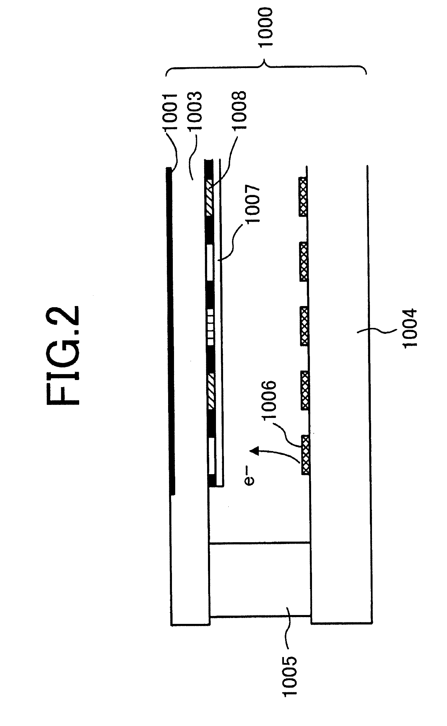
[0106]Next, an image display apparatus according to the second embodiment of the present invention will be described below.

[0107]FIG. 7 shows a partial cross sectional typical view of an image display apparatus according to the second embodiment of the present invention. The basic function of the present embodiment is the same as the constitution shown in the first embodiment, however, a front plate (a third substrate) 1026 is provided with the antireflection function and the functional film to be directly mounted on the face plate does not include the antireflection function. In other words, the front plate (the third substrate) 1026 having the antireflection property is provided on the side of the second face of the second substrate (the face plate) 1003.

[0108]The front plate 1026 is a substrate that is optically transparent and is located on the side of the second face of the second substrate (the face plate) spatially apart from the conductive layer. In other words, the front pl...


PUM


Abstract

There is provided an image display apparatus including: a first substrate having an electron-emitting device; a second substrate having an anode electrode that is opposed to the electron-emitting device; and a conductive layer that is provided on the side of a second face of the second substrate, the second face being an opposite face to a first face of the second substrate, the first face being located on the first substrate side, wherein a potential of the conductive layer is set to be lower than a potential of the anode electrode when displaying an image; and a surface resistance of the conductive layer is higher than a surface resistance of the anode electrode.

Description

BACKGROUND OF THE INVENTION[0001]1. Field of the Invention[0002]The present invention relates to an image display apparatus, a manufacturing method of the image display apparatus, and a functional film.[0003]2. Description of the Related Art[0004]Conventionally, as an electron-emitting device, a cold cathode electron-emitting device has been known. As a cold cathode electron-emitting device, a surface conduction electron-emitting device, a field emission type electron-emitting device (hereinafter, referred to as an FE type electron-emitting device), a metal-insulator-metal type electron-emitting device (hereinafter, referred to as an MIM type electron-emitting device) or the like have been known.[0005]In Japanese Patent Application Laid-Open (JP-A) No. H10 (1998)-326583 (U.S. Pat. No. 6,677,706, EP No. 0866491), and JP-A No. 2003-229079 (U.S. Pat. No. 6,800,995), the applications to the image display apparatus of the surface conduction electron-emitting device and the image display ...

Claims


Application Information

Patent Timeline
IPC IPC(8): H01J1/62H01J9/02
CPCH01J9/20H01J31/127H01J29/085
Inventor DATE, TAKASHIKOIWA, KAORUOGUCHI, TAKAHIROSUZUKI, KEIJI
Owner CANON KK
Why Eureka
Try Eureka