
End point detection method applying resonance phenomenon, end point detection apparatus, chemical mechanical polishing apparatus on which the detection apparatus is loaded, and semiconductor device fabricated by the chemical mechanical polishing apparatus

a technology of resonance phenomenon and detection method, which is applied in the direction of semiconductor/solid-state device testing/measurement, manufacturing tools, and lapping machines, etc., to achieve the effect of preventing excessive polishing or insufficient polishing amount, high accuracy and comparatively low pri

Inactive Publication Date: 2008-07-03
TOKYO SEIMITSU
View PDF5 Cites 5 Cited by
  • Summary
  • Abstract
  • Description
  • Claims
  • Application Information

AI Technical Summary

Benefits of technology

[0015]Secondly, the planar inductor generates a varying primary magnetic field. The planar inductor causes electrostatic induction in the side of the electrically conductive film by the phase difference on the planar inductor, and the planar inductor undergoes electrostatic coupling with the electrically conductive film via the distributed capacitance. The induced current generated in the surface portion of the electrically conductive film upon the electrostatic induction generates a secondary magnetic field in the direction that cancels out the primary magnetic field. The secondary magnetic field acts in the direction that reduces the inductance. Herein, in the region in which the thickness of the electrically conductive film is thin so that the skin effect cannot be ignored, it is considered that the thinner the film thickness, the more the generation amount of the induced current generated in the electrically conductive film is reduced, and the secondary magnetic field is attenuated at the same time. Therefore, reduction in the thickness of the electrically conductive film leads to reduction in the reduction component of the inductance, and the inductance of the sensor circuit system is equivalently increased as a result, thereby reducing the oscillation frequency.
[0061]The invention according to claim 15 is a semiconductor device fabricated in the chemical mechanical polishing apparatus according to claim 14; therefore, the end point detection apparatus having the sensor composed of an oscillation circuit of, for example, the Colpitts type or the like having the planar inductor and the concentrated constant capacitor is loaded in the manner that it is embedded in either the upper surface portion of the platen in the chemical mechanical polishing apparatus or in the polishing head, monitors the variation in the thickness of the electrically conductive film in real time, and can detect the polishing end point, at which the electrically conductive film is polished and removed to an appropriate thickness, at high accuracy. Therefore, there is an advantage that a high-performance semiconductor device can be fabricated.

Problems solved by technology

Secondly, the planar inductor generates a varying primary magnetic field.

Method used


Image

  • End point detection method applying resonance phenomenon, end point detection apparatus, chemical mechanical polishing apparatus on which the detection apparatus is loaded, and semiconductor device fabricated by the chemical mechanical polishing apparatus
  • End point detection method applying resonance phenomenon, end point detection apparatus, chemical mechanical polishing apparatus on which the detection apparatus is loaded, and semiconductor device fabricated by the chemical mechanical polishing apparatus
  • End point detection method applying resonance phenomenon, end point detection apparatus, chemical mechanical polishing apparatus on which the detection apparatus is loaded, and semiconductor device fabricated by the chemical mechanical polishing apparatus

Examples


Embodiment Construction

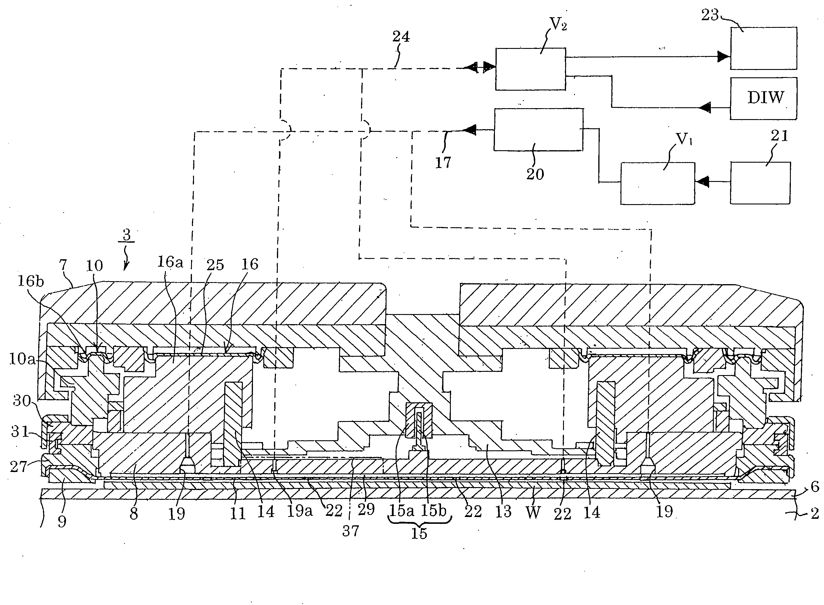
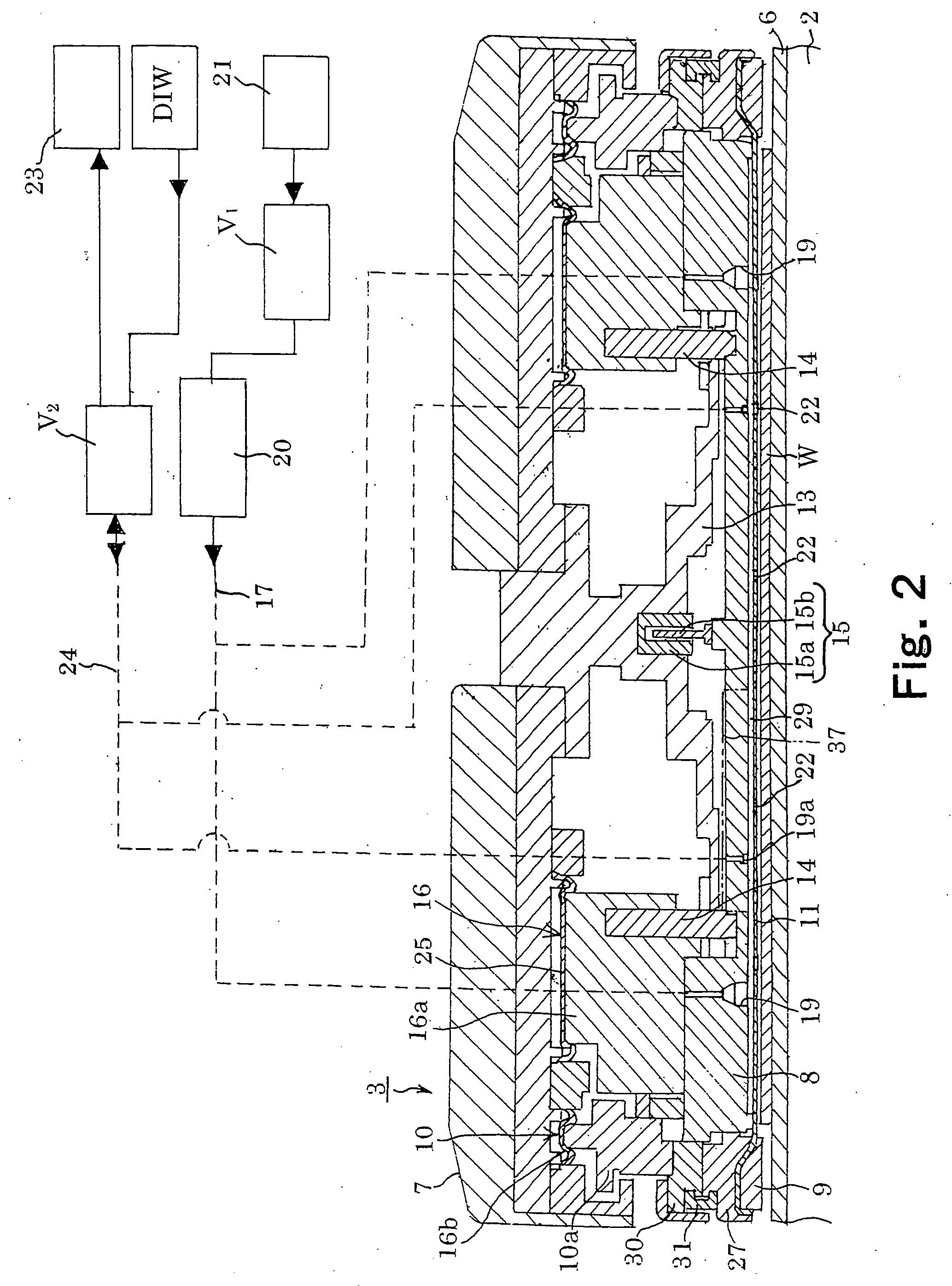
[0074]This is an end point detection method in which an electrically conductive film is polished and a polishing end point at which an appropriate thickness thereof is removed is detected in order to achieve objects of monitoring the variation in the thickness of the electrically conductive film in real time so as to reliably detect the polishing end point of the electrically conductive film at high accuracy, eliminating generation of noise, achieving low power consumption, and reducing the cost. The method is realized by using a sensor composed of an oscillation circuit of the Colpitts type or the like having a planar inductor and a concentrated constant capacitor, monitoring the variation in the thickness of the electrically conductive film in real time from the variation in the oscillation frequency of the sensor caused along with the variation in the thickness of the electrically conductive film opposed to the planar inductor, and detecting the polishing end point based on the p...


PUM

PropertyMeasurementUnit
Frequencyaaaaaaaaaa
Thicknessaaaaaaaaaa
Electrical conductivityaaaaaaaaaa

Abstract

To provide an end point detection method applying a resonance phenomenon, an end point detection apparatus, and a chemical mechanical polishing apparatus on which the detection apparatus is loaded for monitoring variation in the thickness of an electrically conductive film in real time, reliably detecting a polishing end point of the electrically conductive film at high accuracy, without generating noise, low power consumption, and capable of reducing the cost.In order to achieve above described objects, the present invention provides an end point detection method applying a resonance phenomenon in which a polishing end point is detected when the electrically conductive film is polished and removed to an appropriate thickness, wherein a sensor 37 composed of an oscillation circuit of the Colpitts type or the like having a planar inductor and a concentrated constant capacitor is used, and the variation in the thickness of the electrically conductive film is monitored in real time from the variation in the oscillation frequency of the sensor 37 caused along with the variation in the thickness of the electrically conductive film opposed to the planar inductor.

Description

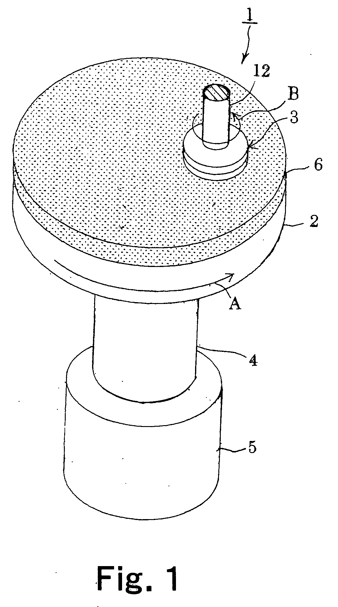
FIELD OF THE INVENTION[0001]The present invention relates to an end point detection method applying a resonance phenomenon, an end point detection apparatus, a chemical mechanical polishing apparatus on which the detection apparatus is loaded, and a semiconductor device fabricated by the chemical mechanical polishing apparatus, and particularly relates to an end point detection method applying the resonance phenomenon capable of reliably detecting a polishing end point of an electrically conductive film at high accuracy in chemical mechanical polishing processing (CMP), an end point detection apparatus, a chemical mechanical polishing apparatus on which the detection apparatus is loaded, and a semiconductor device fabricated by the chemical mechanical polishing apparatus.BACKGROUND OF THE INVENTION[0002]As a conventional art related to an end point detection method applying the resonance phenomenon, an end point detection apparatus, and a chemical mechanical polishing apparatus on w...

Claims


Application Information

Patent Timeline
IPC IPC(8): C23F1/00B24B37/013H01L21/304
CPCB24B37/013H01L22/26H01L2924/0002H01L2924/00H01L21/304
Inventor KITADE, KEITAMATSUSHITA, OSAMUFUJITA, TAKASHIYOKOYAMA, TOSHIYUKI
Owner TOKYO SEIMITSU
Learn More