Liquid crystal display device and manufacturing method for the same

a technology of liquid crystal display and manufacturing method, which is applied in non-linear optics, instruments, optics, etc., can solve problems such as abnormal display with trace of misalignment, and achieve the effects of improving display quality, poor display, and increasing transmittan

Active Publication Date: 2008-06-26
JAPAN DISPLAY WEST
View PDF8 Cites 3 Cited by
  • Summary
  • Abstract
  • Description
  • Claims
  • Application Information

AI Technical Summary

Benefits of technology

[0013]It is thus desirable to suppress the degree of misalignment to be occurred to liquid crystal molecules as a result of a push on the display surface of a liquid crystal display device, i.e., surface push, by making sub-pixels as a result of pixel division to make those to serve each as an electrically independent pixel.
[0015]In the embodiment of the invention, the provision of a dielectric member on a portion of electrical connection among sub-pixels enables to electrically separate the sub-pixels from one another so that liquid crystal molecules can be aligned stably. As such, even if the alignment of the liquid crystal molecules is once lost due to a push on a liquid crystal panel, the alignment is soon recovered back to the former state thereof, thereby favorably solving the problem of poor display with a trace as a result of the surface push on the liquid crystal panel.
[0017]In the this embodiment of the invention, the provision of a step of forming a dielectric member on a portion of electrical connection among sub-pixels enables to electrically separate the sub-pixels from one another so that liquid crystal molecules can be aligned stably. As such, even if the alignment of the liquid crystal molecules is once lost due to a push on a liquid crystal panel, the alignment is soon recovered back to the former state thereof, thereby favorably providing a liquid crystal display device causing no problem of poor display with a trace as a result of the surface push on the liquid crystal panel.
[0018]With the embodiments of the invention, there are advantages of being able to improve the display quality because there is no more possibility of poor display that has been caused by a surface push on a liquid crystal panel. Further, the size minimization is achieved to a dielectric member formed on a portion of electrical connection among sub-pixels and an alignment control element formed to each of the sub-pixels for alignment control over liquid crystal molecules, thereby being able to increase the transmittance. Still further, because the resistance against a surface push is improved, there is no more need to reduce the space between substrates, i.e., so-called cell gap, that has been required for improving the resistance against the surface push. This thus enables to increase the space between the substrates so that the properties of transmittance can be improved.
[0019]With the embodiments of the invention, there are advantages of being able to provide a liquid crystal display deice with which the display quality is improved because there is no more possibility of poor display that has been caused by a surface push on a liquid crystal panel. Further, the size minimization is achieved to a dielectric member formed on a portion of electrical connection among sub-pixels and an alignment control element formed to each of the sub-pixels for alignment control over liquid crystal molecules, thereby being able to provide a liquid crystal display device with which the transmittance is increased. Still further, because the resistance against a surface push is improved, there is no more need to reduce the space between substrates, i.e., so-called cell gap, that has been required for improving the resistance against the surface push. This thus enables to provide the liquid crystal display device with which the space can be increased between the substrates so that the properties of transmittance can be improved.

Problems solved by technology

When the alignment of liquid crystal molecules is once lost with a push on a liquid crystal panel, for example, the alignment is never recovered back to the former condition, thereby resulting in abnormal display with a trace of misalignment on the liquid crystal panel.

Method used


Image

  • Liquid crystal display device and manufacturing method for the same
  • Liquid crystal display device and manufacturing method for the same
  • Liquid crystal display device and manufacturing method for the same

Examples


first embodiment

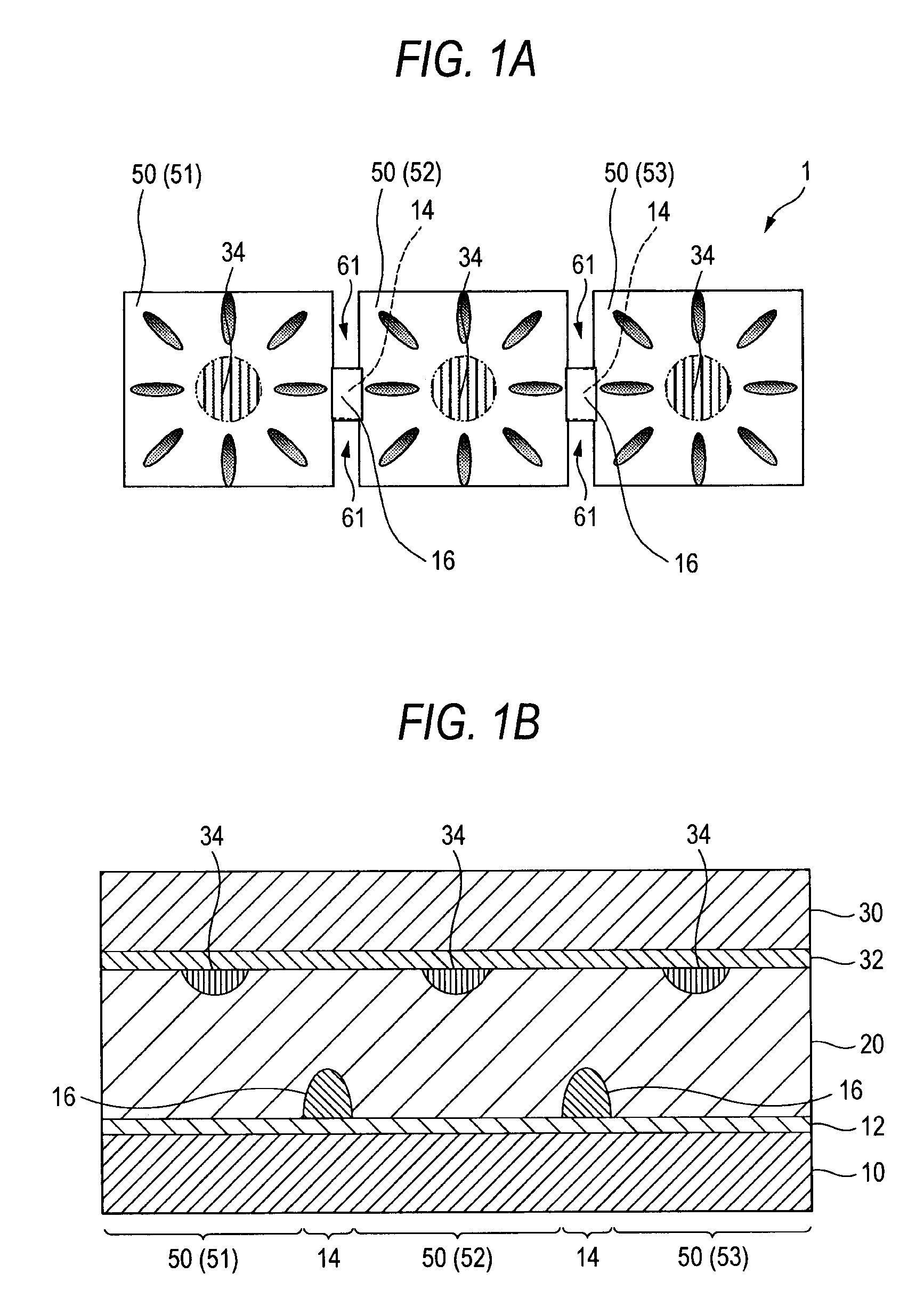
[0032]By referring to a schematic plan layout of FIG. 1A and a main-part cross sectional view of FIG. 1B, described is an embodiment, i.e., first embodiment, of the invention.

[0033]As shown in FIGS. 1A and 1B, the liquid crystal material of a liquid crystal display device 1 is of a vertical alignment type. In the device, a liquid crystal layer 20 is sealed between opposing substrates 10 and 30, and a plurality of pixels 40 are included for image display. The pixels 40 are each configured by a plurality of sub-pixels 50, e.g., sub-pixels 51, 52, and 53, which are alignment-divided. The sub-pixels 50 are electrically connected to one another by a pixel electrode 12 formed on the substrate 10, and the pixel electrode 12 between the sub-pixels 50 is formed with a notch 61, for example. The pixel electrode 12 between the sub-pixels 50 is formed thereon with a dielectric member 16, and such a portion is hereinafter referred to as connection portion 14.

[0034]The pixel division for alignmen...

second embodiment

[0042]By referring to the schematic plan layout of FIG. 4A showing the positional relationship between a pixel electrode and an alignment control element, and another schematic plan layout of FIG. 4B showing the positional relationship between a pixel electrode and a dielectric member, described next is an embodiment, i.e., a second embodiment, of the invention.

[0043]As shown in FIG. 4A, the connection portion 14 of the pixel electrode 12 is formed to the vertical end portions between any two sub-pixels 50. As shown in FIG. 4B, by forming the dielectric member 16 to the connection portion 14, this configuration also leads to the effect similar to that of the configuration of the dielectric member 16A described by referring to Table 1.

third embodiment

[0044]By referring to the schematic plan layout of FIG. 5A showing the positional relationship between a pixel electrode and an alignment control element, and another schematic plan layout of FIG. 5B showing the positional relationship between a pixel electrode and a dielectric member, described is an embodiment, i.e., a third embodiment, of the invention.

[0045]As shown in FIG. 5A, the connection portion 14 of the pixel electrode 12 is formed entirely to the portion between any two sub-pixels 50. As shown in FIG. 5B, by forming the dielectric member 16 on the connection portion 14, this configuration also leads to the effect similar to that of the configuration of the dielectric member 16A described by referring to Table 1.

[0046]As such, by forming the dielectric member 16 on the pixel electrode 12 (connection portion 14) where the sub-pixels are electrically connected irrespective of the formation position of the connection portion 14, the test result shows that the alignment of th...


PUM

PropertyMeasurementUnit
weightaaaaaaaaaa
electric fieldsaaaaaaaaaa
electrical connectionaaaaaaaaaa

Abstract

A liquid crystal display device is disclosed. The liquid crystal display includes a liquid crystal layer disposed between substrates opposing each other. A pixel of the liquid crystal display is alignment-divided into a plurality of sub-pixels. A dielectric member is provided on a connection portion where the sub-pixels are electrically connected.

Description

CROSS REFERENCES TO RELATED APPLICATIONS[0001]The present invention contains subject matter related to Japanese Patent Application JP 2006-342140 filed in the Japanese Patent Office on Dec. 20, 2006, the entire contents of which being incorporated herein by reference.BACKGROUND OF THE INVENTION[0002]1. Field of the Invention[0003]The present invention relates to a liquid crystal display device and a manufacturing method for the same.[0004]2. Description of the Related Art[0005]As is advantageously slim, light in weight, and low in power consumption, a liquid crystal display device has been popular as a display device being applicable to various many uses. The liquid crystal display device is recently used widely, including a large-sized television receiver for home use and a small-sized mobile phone, and thus the demand for the properties of the display device, especially the demand for the viewing angle thereof is getting tough.[0006]In consideration thereof, proposed are previous ...

Claims


Application Information

Patent Timeline
Patent Type & Authority Applications(United States)
IPC IPC(8): G02F1/1333G02F1/13
CPCG02F1/133707G02F2001/134345G02F1/13394G02F1/133753G02F1/134345G02F1/1337
Inventor KOITO, TAKEOKATAOKA, SHINGOSAKAI, EIJINISHIKAWA, HIROSHI
Owner JAPAN DISPLAY WEST
Why Eureka
Try Eureka