Display device

Active Publication Date: 2008-06-12
UDC IRELAND
View PDF14 Cites 15 Cited by
  • Summary
  • Abstract
  • Description
  • Claims
  • Application Information

AI Technical Summary

Benefits of technology

[0020]According to the first and second aspects of the invention, the display device includes a first electrode and a second electrode which are respectively disposed in intersecting directions on or above a flexible substrate. The flexible substrate may be substantially rectangular. A display pixel is formed at an area of overlap between the two electrodes in a direction substantially perpendicular to the plane of the electrodes. The first electrode and the second electrode are respectively connected to flexible wiring members at a first region of a periphery of the flexible substrate and a second region adjacent to the first region. One of the flexible wiring members is adhered onto a display unit, the flexible wiring member connected to the second region is drawn out to the first region, and connection portions of two flexible wiring members are disposed at the same region as the first region at the periphery of the flexible substrate, similarly to the flexible wiring member connected to the first region, and may be connected externally. As a result, in the flexible display, the wirings are drawn out at only one region, and the dead space of the substrate is reduced, which is particularly advantageous in a hand-held display device.
[0048]According to the invention, the flexible wiring members are adhered onto the display unit, the second flexible wiring member, which out of the adjacent first region and second region on the periphery of the flexible substrate is connected to the second region, is drawn out to the first region of the flexible substrate, and is projected from the end of the first region of the flexible substrate similarly to the first flexible wiring member that is connected to the first region, and hence the two flexible wiring members are connected at one region, and the flexible wiring members are assembled at one region at a periphery of the flexible substrate, and, spatially, dead space additional to the display unit is eliminated.

Problems solved by technology

Solutions for accomplishing miniaturization and reduction of weight are disclosed in Japanese Patent Application Laid-Open (JP-A) Nos. 2002-82627 and 2003-17245, but the problems have not been solved sufficiently thus far.
However, since it is generally difficult to manufacture a flexible thin film transistor (TFT) that exhibits sufficient performance on a flexible substrate such as polyethylene naphthalate (PEN), the passive matrix drive mode is expected to be an effective driving mode.
However, in the case of control by the passive matrix drive mode, the amount of wiring to be connected to an external drive circuit is larger than when the active matrix drive mode is used.
The passive matrix drive mode is an effective driving method for a flexible display, but it requires a large amount of connecting wiring for driving, and a large space is required for the wiring.

Method used


Image

  • Display device
  • Display device
  • Display device

Examples


first exemplary embodiment

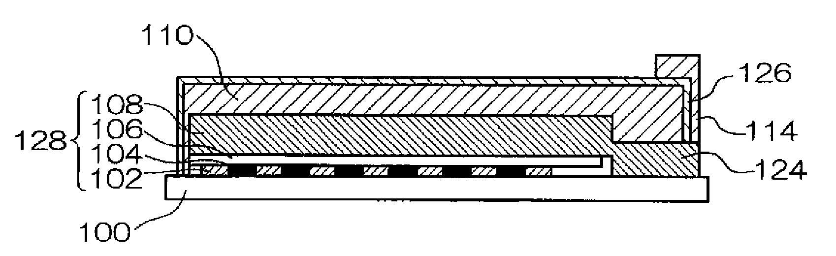
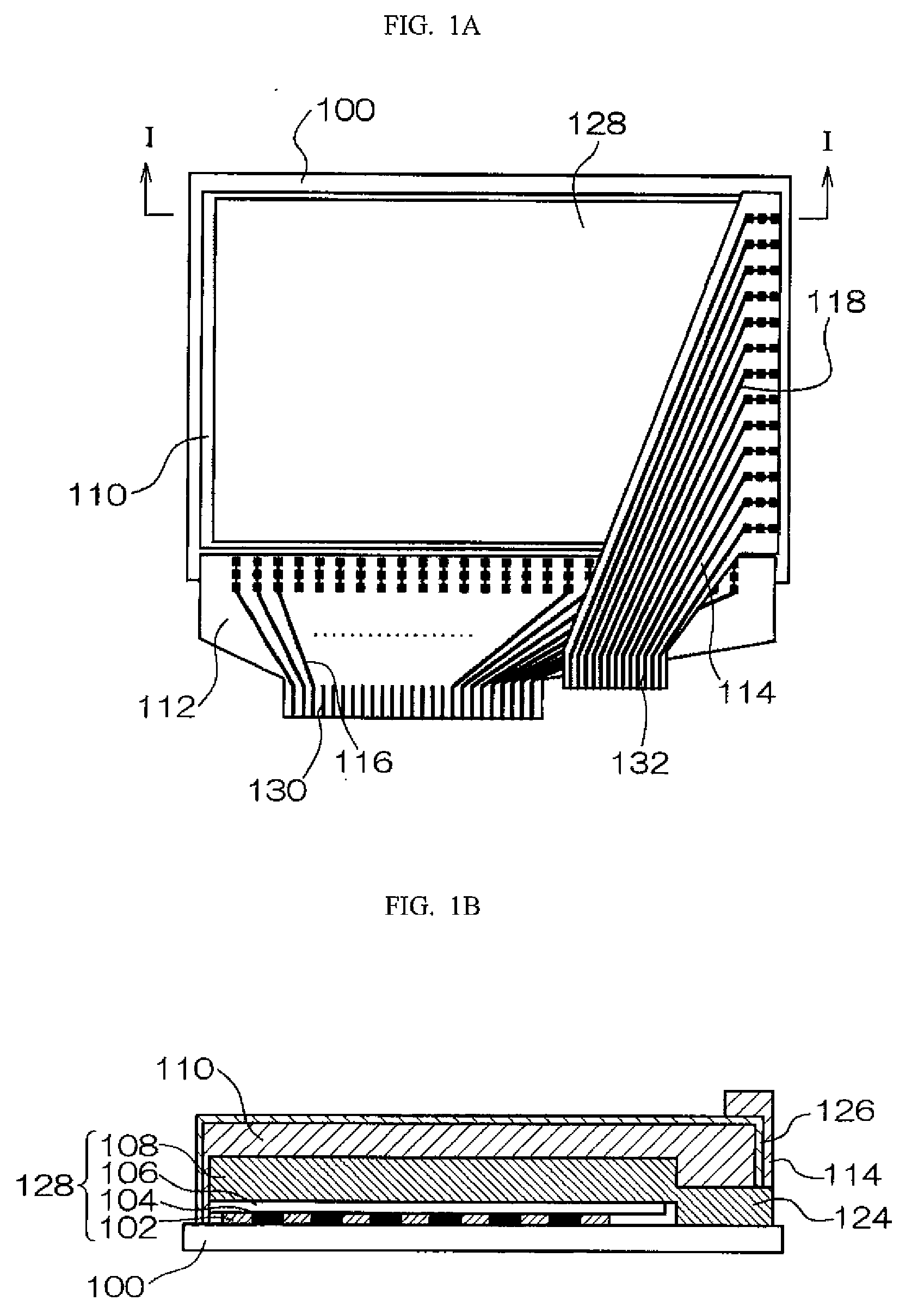
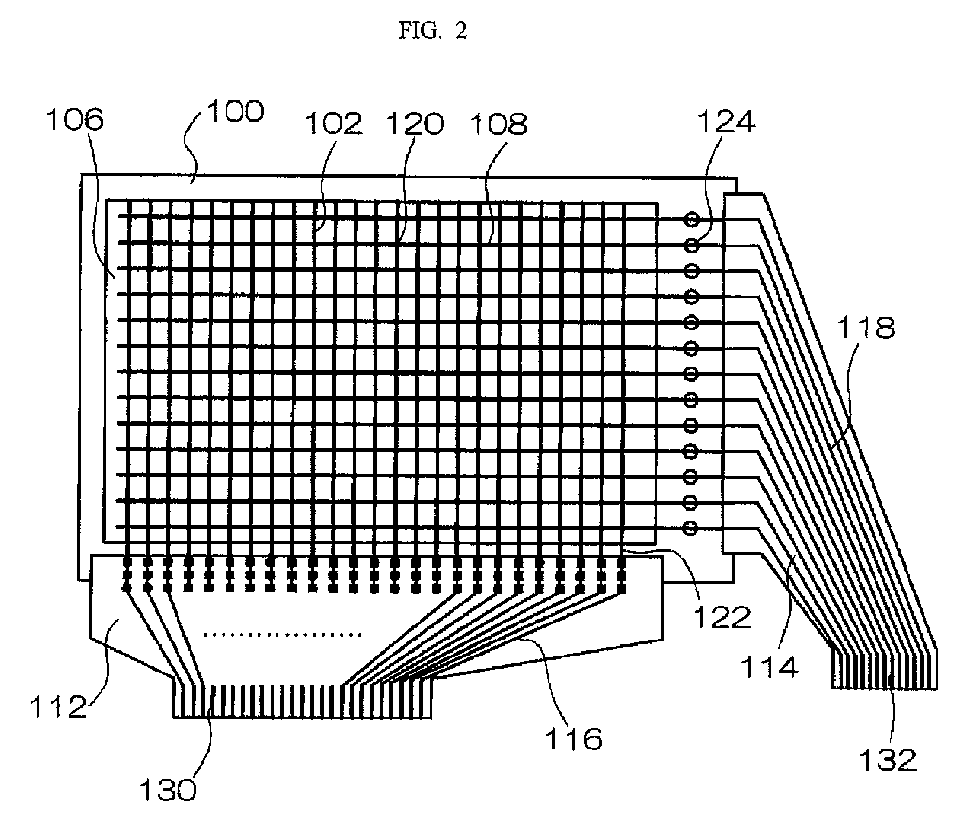
[0059]FIG. 1A is a plan view showing a first exemplary embodiment of the invention. FIG. 1B is a sectional view of the first exemplary embodiment taken along the line I-I in FIG. 1A, and FIG. 2 is an explanatory diagram showing the layout of the wiring in FIG. 1A.

[0060]On a substantially rectangular flexible substrate 100, Faust electrodes 102 each having a strip shape are disposed in a row to form line electrodes. An organic layer 106 including an organic compound, such as a light emitting layer, is laminated on the first electrodes 102. Second electrodes 108 each having a strip shape are disposed in a row on the organic layer 106 in a direction intersecting that of the first electrodes 102 such that the organic layer 106 is interposed between the first electrodes 102 and the second electrodes 108, the second electrodes 108 forming line electrodes. Each rectangular area of overlap between the first electrodes 102 and the second electrodes 108 in a direction substantially perpendicu...

second exemplary embodiment

[0066]FIG. 3A shows the second exemplary embodiment of the invention in which the second electrode 108 shown in FIG. 1 showing the first exemplary embodiment is divided into two sections on the display unit, and the display unit 128, which is driven by one system in the first exemplary embodiment, is driven by two systems. FIG. 3A shows a plan view of an organic EL panel using an organic compound in the optical functional layer, and FIG. 4 shows the wirings shown in FIG. 3A.

[0067]On a flexible substrate 200, first electrodes 202 each having a strip shape are disposed in a row to form line electrodes. An organic layer 206 including an organic compound, such as a light emitting layer is laminated on the first electrodes 202. Second electrodes 208 and third electrodes 210, each of which has a strip shape, are disposed on the organic layer 206 in a row in a direction intersecting with that of the first electrodes 202 such that the organic layer 206 is interposed between the first electr...

third exemplary embodiment

[0073]FIG. 5A shows the third exemplary embodiment of the invention which is the same as the first exemplary embodiment except that the first electrode 102 in FIG. 1 is divided into two sections on the display unit, and the display unit 128, which is driven by one system in the first exemplary embodiment, is driven by two systems in the third exemplary embodiment. FIG. 5A shows a plan view of an organic EL panel using an organic compound in the optical functional layer, and FIG. 6 shows the wiring shown in FIG. 5A.

[0074]On a flexible substrate 300, first electrodes 302 and fourth electrodes 304 each having a strip shape are disposed in a row to each form line electrodes. An organic layer 308 including an organic compound such as a light emitting layer is laminated on the first electrodes 302 and the fourth electrodes 304. Second electrodes 310 each having a strip shape are disposed in a row on the organic layer 308 in a direction intersecting with that of the first electrodes 302 or...


PUM


Abstract

The invention provides a display device including: a first electrode and a second electrode which are disposed in different directions from each other on a flexible substrate; an optical functional layer disposed between the first and second electrodes; and a display unit having a display pixel formed at a rectangular area of overlap between the first and second electrodes in the direction of lamination of the electrodes, in which the first and second electrodes are respectively connected to a first flexible wiring member at a first region of a periphery of the flexible substrate and a second flexible wiring member at a second region adjacent to the first region, one of the first and second flexible wiring members is adhered onto the display unit, and a first connection portion and a second connection portion for connecting the flexible wiring members with external drive units are disposed at the same region on the periphery of the flexible substrate.

Description

CROSS-REFERENCE TO RELATED APPLICATION[0001]This application claims priority under 35 USC 119 from Japanese Patent Application No. 2006-334407, the disclosure of which is incorporated by reference herein.BACKGROUND OF THE INVENTION[0002]1. Field of the Invention[0003]The present invention relates to a display device having a functional element formed on a flexible substrate. More specifically, the present invention relates to a display device preferably used in a passive matrix drive mode.[0004]2. Description of the Related Art[0005]As a next-generation display or a next-generation device, paper-like flexible displays and flexible lighting have begun to receive considerable attention, which displays or devices are realized by laminating a transparent electrode, an optical functional layer including an organic light emitting element or a liquid crystal element, and a back electrode on a transparent and flexible substrate, and forming a plurality of display pixels. These flexible disp...

Claims


Application Information

Patent Timeline
IPC IPC(8): G06F1/16
CPCG06F1/1601
Inventor TADA, HIROSHI
Owner UDC IRELAND
Why Eureka
Try Eureka