
System and method for automatic elimination of voltage drop, also known as IR drop, violations of a mask layout block, maintaining the process design rules correctness

Inactive Publication Date: 2008-05-29
MICROLOGIC DESIGN AUTOMATION
View PDF3 Cites 38 Cited by
  • Summary
  • Abstract
  • Description
  • Claims
  • Application Information

AI Technical Summary

Benefits of technology

[0020]In accordance with the present invention, the disadvantages and problems associated with eliminating voltage drop violations of a mask layout block have been substantially reduced or eliminated. In a particular embodiment, a method for eliminating voltage drop violations of a mask layout block includes automatic correction of voltage drop violations within mask layout block if identified, maintaining the process design rules (DRC Clean) and layout connectivity (LVS Clean) correctness.
[0025]Important technical advantages of certain embodiments of the present invention include a voltage drop Auto Correct (IR Drop Auto Correct) tool that automatically corrects voltage drop violations of a mask layout block while maintaining the process design rules (DRC Clean) and layout connectivity (LVS Clean) correctness. A layout designer may execute an IC layout block with voltage drop violations. The IR Drop Auto Correct tool highlights a violation marker that may represent a width, space or length in the layout block and eliminates the voltage drop violation according to technology or external constraints file. In addition the IR Drop Auto Correct tool provides an information window with the current and fixed voltage drop conditions related to the selected polygon or signal. The correction action may change polygon's width, length or space according to voltage drop rules taken from technology or external constraints file while maintaining the process design rules (DRC Clean) and layout connectivity (LVS Clean) correctness. In case of contacts or vias individual or multiple selections, the system will automatically adjust the amount of contacts or vias according to voltage drop rules taken from technology or external constraints file. The processed mask layout block, therefore, may be free of voltage drop violations.
[0026]Another important technical advantage of certain embodiments of the present invention includes IR Drop Auto Correct tool that significantly reduces the design time for an integrated circuit. In a typical integrated circuit design process, a voltage drop check (IR Drop Check) tool analyzes a mask layout file for voltage drop violations and identifies any violations in an output file. A layout designer may use the output file to manually eliminate the identified voltage drop violations. Then the same IC layout block needs to be re-checked for voltage drop again and also other checks like reliability (Electromigration & self heat), DRC (Design Rule Check) and LVS (Layout vs. Schematics) to make sure that the connectivity and geometrical sizes are still correct according to technology file and schematics respectfully. These repeated cycles are time consuming and tedious procedures that can be eliminated using the presented invention.
[0027]The time needed to complete the entire design process for the integrated circuit, therefore, may be substantially reduced since the steps of checking the layout with an IR Drop tool and manually correcting the identified voltage drop violations may be eliminated using the automated software as described in this invention.

Problems solved by technology

The current densities (current per cross-sectional area) in the signal lines and power are consequently high and can result in either signal or power electromigration problems.
As modern day ICs become increasingly more powerful, their internal circuitry become increasingly more complex.
Post-layout simulation usually requires a long time to complete, typically taking several days to finish.
Results from this simulation can reveal problems such as excessive power-bus voltage drop and electromigration, which are generally not discoverable during pre-layout simulation.
Voltage drop problems are a result of a large drop in voltage across a wire conducting an electric current.
A large voltage drop across a power-bus wire can cause a lower than desired level of voltage at a particular point in the IC.
This skews circuit timings and may lead to IC malfunctions if time critical operations are not performed when expected.
If the voltage drop across the power-bus wire is even more severe, the logic errors may occur and the entire IC may not operate as expected.
Electromigration is caused when electrons flowing through a wire randomly collide into the atoms of the wire, “carrying” the atoms along their path and causing wire deterioration, much like ocean currents carry beach sand and cause beach erosion.
Electromigration typically leads to voltage drop across a wire, and eventually to a break in the wire.
One drawback of discovering voltage drop and electromigration problems after post-layout simulation relates to the amount of time required for the simulation to complete.
There are often strong market pressures to design and manufacture a new IC in a very short time.
Such problems may add days, if not weeks to the design cycle time and can significantly decrease a product's competitive advantage.
In addition, the post-layout simulation time makes testing and comparing several different power-bus grid designs extremely time consuming.
These conservative estimates generally result in power-bus wire widths which are significantly thicker than actually necessary to supply power throughout the IC core.
A drawback of over-estimating circuit power requirements is a sub-optimal use of the IC's available silicon core space.
Thus, power-bus wires designed thicker than actually needed tend to waste valuable room on the IC.

Method used


Image

  • System and method for automatic elimination of voltage drop, also known as IR drop, violations of a mask layout block, maintaining the process design rules correctness
  • System and method for automatic elimination of voltage drop, also known as IR drop, violations of a mask layout block, maintaining the process design rules correctness
  • System and method for automatic elimination of voltage drop, also known as IR drop, violations of a mask layout block, maintaining the process design rules correctness

Examples


Embodiment Construction

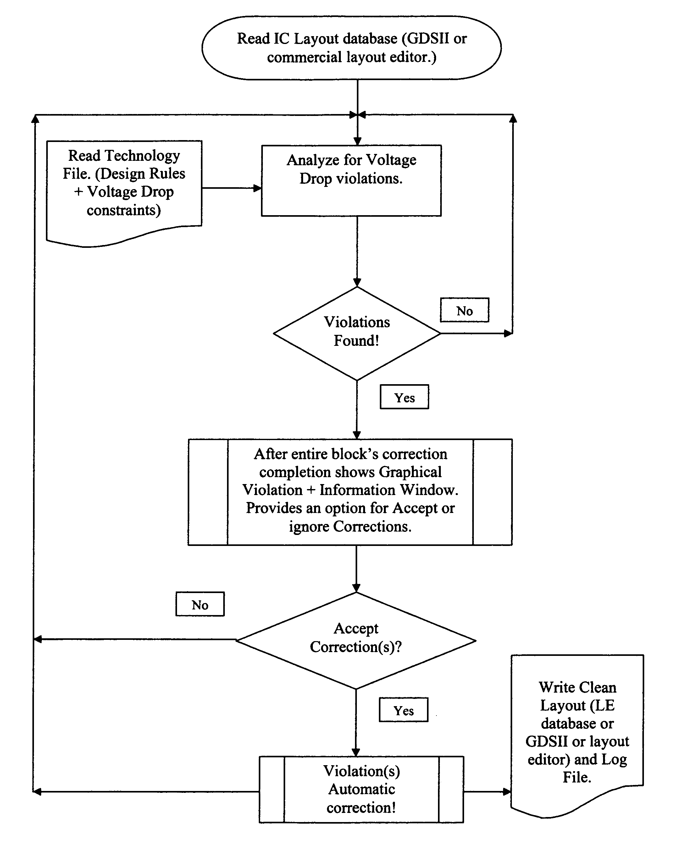
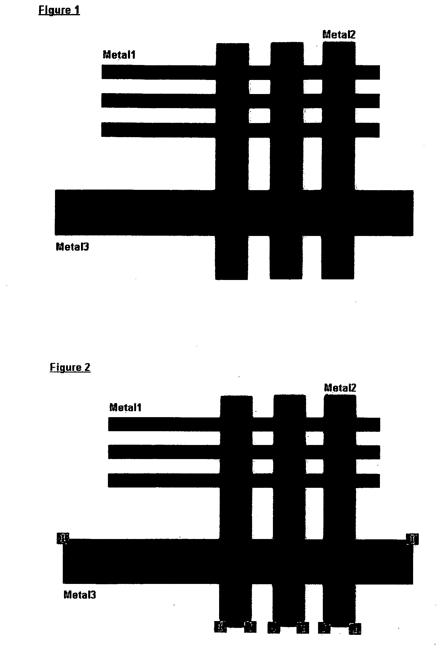
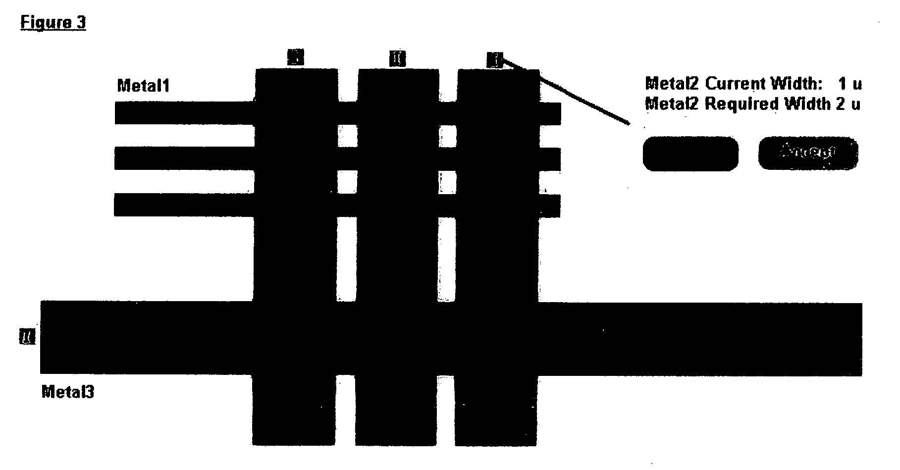
[0037]The processing instructions may include a commercially available layout editor interfaced with a voltage drop Auto correct (IR Drop Auto Correct) tool or an independent IC layout block in GDSII format or any other commercial format database. The IR Drop Auto Correct tool may provide the ability to analyze the width, length and placement of polygons in a mask layout block and determine if a voltage drop violation was created. In addition the IR Drop Auto Correct tool may provide the ability to analyze the number of contacts and VIA's, determine the amount needed in order to comply with voltage drop requirements. The IR Drop Auto Correct tool may automatically correct all voltage drop violation maintaining the process design rules (DRC Clean) and layout connectivity (LVS Clean) correctness.

[0038]After a layout designer creates a mask layout block it may contain voltage drop violations. The IR Drop Auto Correct tool reads the layout block information from GDSII format file or fro...


PUM


Abstract

A system and method for automatic correction of voltage drop, also known as IR Drop violations of a mask layout block, maintaining the process design rules (DRC Clean) and layout connectivity (LVS Clean) correctness, are disclosed. The method includes analyzing polygons or signals for voltage drop violations, in a mask layout block and obtaining one or more voltage drop restriction information associated with polygons or signals from a technology and an external constraints file. The system automatically corrects all voltage drop violations if found, changing polygons space, width and length, maintaining the process design rules (DRC Clean) and layout connectivity (LVS Clean) correctness. The method also includes analysis and automatic correction of contacts and VIA's according to amount and location in order to comply with voltage drop requirements as taken from technology or external constraints file. The method provides a violation marker associated with position of polygons or signals that graphically represents a width, space, length violation. The method and system works on GDSII format files and on industry standards layout editor's database.

Description

BACKGROUND OF INVENTION[0001]1. Technical Field of the Invention[0002]The present invention is generally related to the field of integrated circuits, and more particularly to a system and method for automatic correction of voltage drop violations within a mask layout block in the metallic, polysilicon, contacts and VIA's interconnects of an integrated circuit device, maintaining the process design rules (DRC Clean) and layout connectivity (LVS Clean) correctness.[0003]2. Background of the Invention[0004]Nanometer designs contain millions of devices and operate at very high frequencies. The current densities (current per cross-sectional area) in the signal lines and power are consequently high and can result in either signal or power electromigration problems. Microelectronic integrated circuits (ICs), such as computer chips, are used in a variety of products including personal computers, automobiles, communication systems, and consumer electronics products. As modern day ICs become ...

Claims


Application Information

Patent Timeline
IPC IPC(8): G06F17/50
CPCG06F17/5068G06F17/5036G06F30/367G06F30/39
Inventor RITTMAN, DAN
Owner MICROLOGIC DESIGN AUTOMATION
Learn More