Semiconductor package substrate and method, in particular for MEMS devices

a technology of semiconductors and substrates, applied in the direction of microstructural devices, electrical apparatus construction details, microstructures, etc., can solve the problems of loss of sealing effect, relative fragility and brittleness, high stress conditions of mounted dice, etc., to achieve less susceptible to damage, less mechanical stability, and performance quality and durability.

Active Publication Date: 2008-04-17
STMICROELECTRONICS SRL
View PDF3 Cites 0 Cited by
  • Summary
  • Abstract
  • Description
  • Claims
  • Application Information

AI Technical Summary

Benefits of technology

[0038]It has been found, in fact, that by forming metal support zone patterns according to aspects of the invention, the package substrate is considerably more balanced throughout the manufacturing assembly steps, so that the device is less exposed to delamination, warpage, and the mechanical and thermal stresses which c

Problems solved by technology

Since the material of a semiconductor wafer—commonly silicon—tends to be relatively fragile and brittle, dice are usually assembled into protective housings, or “packages,” before being interconnected with a printed circuit board (PCB), the package ensuring the interconnection between the dice and the board.
The package, in fact, can undergo considerable mechanical stress during manufacturing, especially during the molding step, which can lead to tilting of the die and failure by delamination of its cap, with consequent loss of the sealing effect, which in turn affects the durability of the device as well as its quality of performance, in terms of offset stability and

Method used


Image

  • Semiconductor package substrate and method, in particular for MEMS devices
  • Semiconductor package substrate and method, in particular for MEMS devices
  • Semiconductor package substrate and method, in particular for MEMS devices

Examples


Embodiment Construction

[0051]The following discussion is presented to enable a person skilled in the art to make and use the invention. Various modifications to the embodiments will be readily apparent to those skilled in the art, and the generic principles herein may be applied to other embodiments and applications without departing from the spirit and scope of the present invention. Thus, the present invention is not intended to be limited to the embodiments shown, but is to be accorded the widest scope consistent with the principles and features disclosed herein.

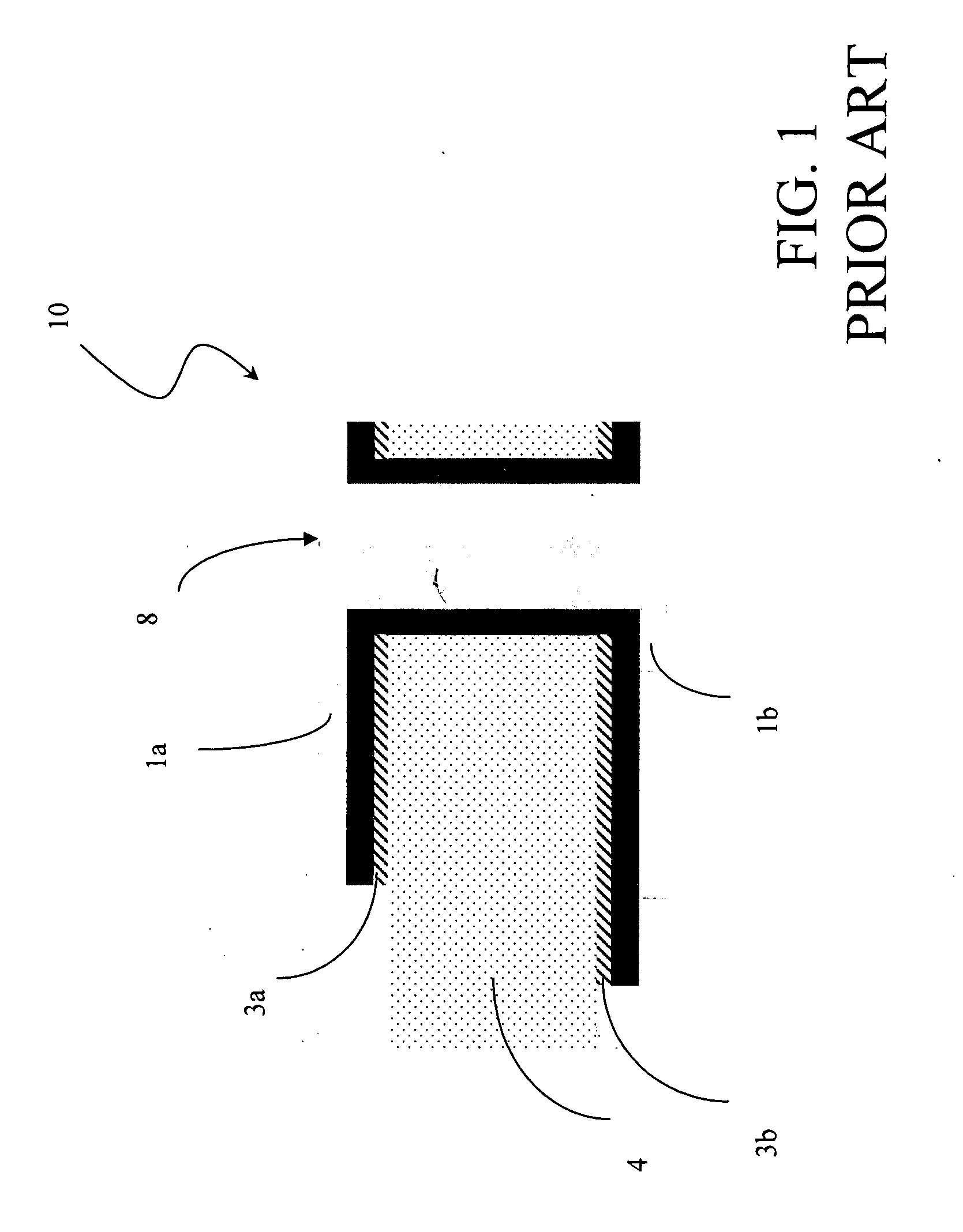
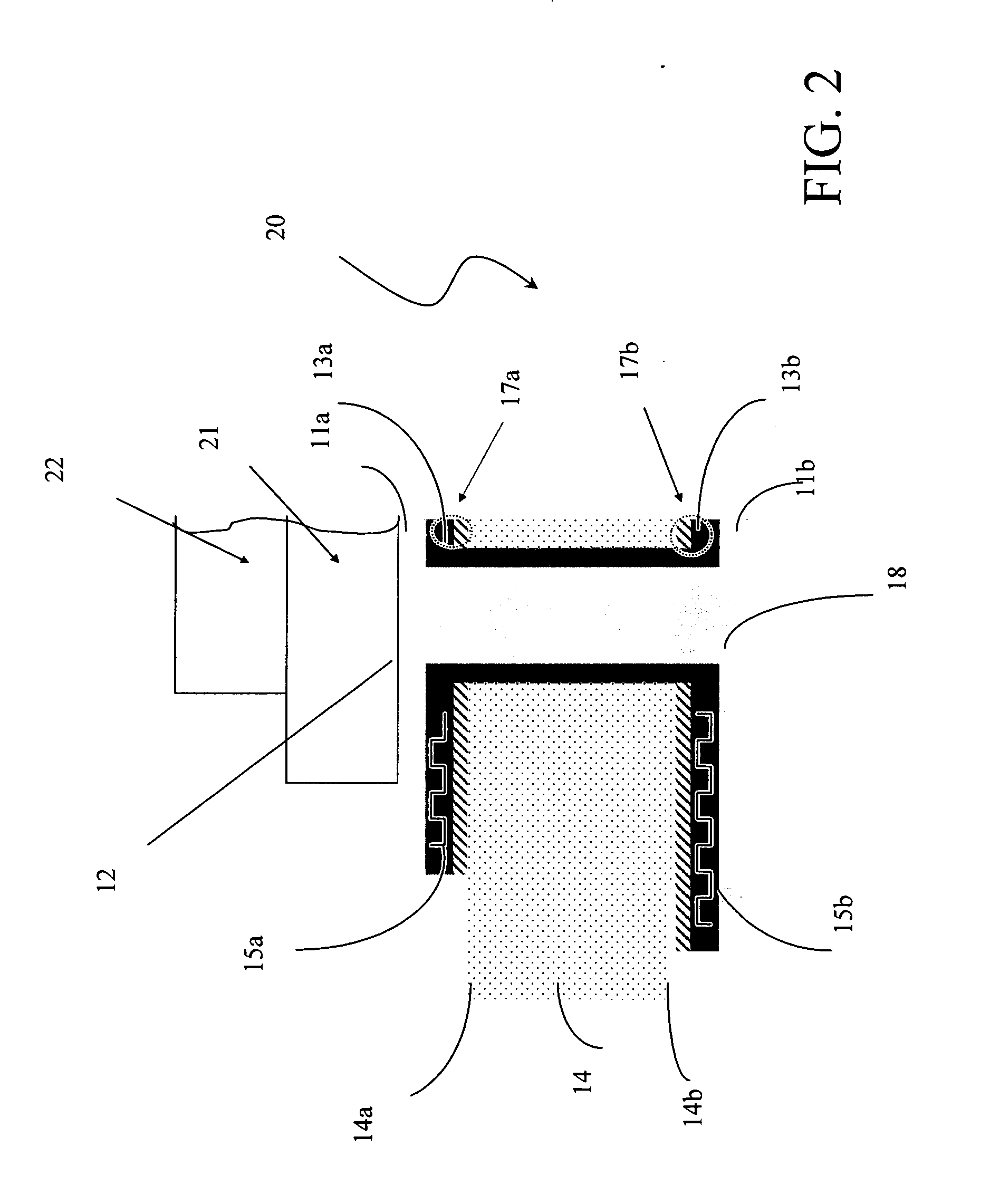
[0052]With reference to such figures, and in particular with reference to FIGS. 2 to 4, a package substrate according to an embodiment of the invention, referred to in its entirety by reference number 20, will now be described in greater detail also by means of two representative examples shown in FIGS. 3 and 4, concerning package substrates intended to support damage-sensitive devices, such as MEMS devices.

[0053]Features of embodiments of the ...


PUM


Abstract

A semiconductor package substrate suitable for supporting a damage-sensitive device, including a substrate core having a first and opposite surface; at least one pair of metal layers covering the first and opposite surfaces of the package substrate core, which define first and opposite metal layer groups, at least one of said layer groups including at least one metal support zone; one pair of solder mask layers covering the outermost metal layers of the at least one pair of metal layers; and a plurality of routing lines; wherein the at least one metal support zone is formed so that it lies beneath at least one side of the base of the damage-sensitive device and so as to occupy a substantial portion of the area beneath the damage-sensitive device which is free of said routing lines; a method for the production of such substrate is also described.

Description

BACKGROUND OF THE INVENTION[0001]1. Field of the Invention[0002]The present invention generally relates to a semiconductor package substrate and manufacturing methods thereof.[0003]More in particular, but not exclusively, the present invention relates to a land grid array (LGA) and ball grid array (BGA) semiconductor package substrate supporting a micro-electro-mechanical system (MEMS) device, and the following description is made with reference to such a specific technical field for the sole purpose of simplifying the disclosure of the invention.[0004]2. Background of the Invention[0005]As it is well known, a micro-electro-mechanical system (MEMS) device is a microdevice that integrates mechanical and electrical functions in a silicon chip realized using lithographic microfabrication techniques.[0006]The final assembled device or chip is typically composed of a MEMS die and optionally application-specific integrated circuits (ASICs) assembled on top of a substrate both in side by s...

Claims


Application Information

Patent Timeline
IPC IPC(8): H01L23/02
CPCB81B7/0048B81B2207/07H01L23/3121H01L23/49838H01L23/562H01L2924/1433H01L2924/0002H01L2924/3511H05K1/0271H01L2924/00
Inventor ZIGLIOLI, FEDERICOGRAZIOSI, GIOVANNICORTESE, MARIO
Owner STMICROELECTRONICS SRL
Why Eureka
Try Eureka