
Process for manufacturing process of semiconductor device

Active Publication Date: 2008-03-20
LINTEC CORP
View PDF17 Cites 8 Cited by
  • Summary
  • Abstract
  • Description
  • Claims
  • Application Information

AI Technical Summary

Benefits of technology

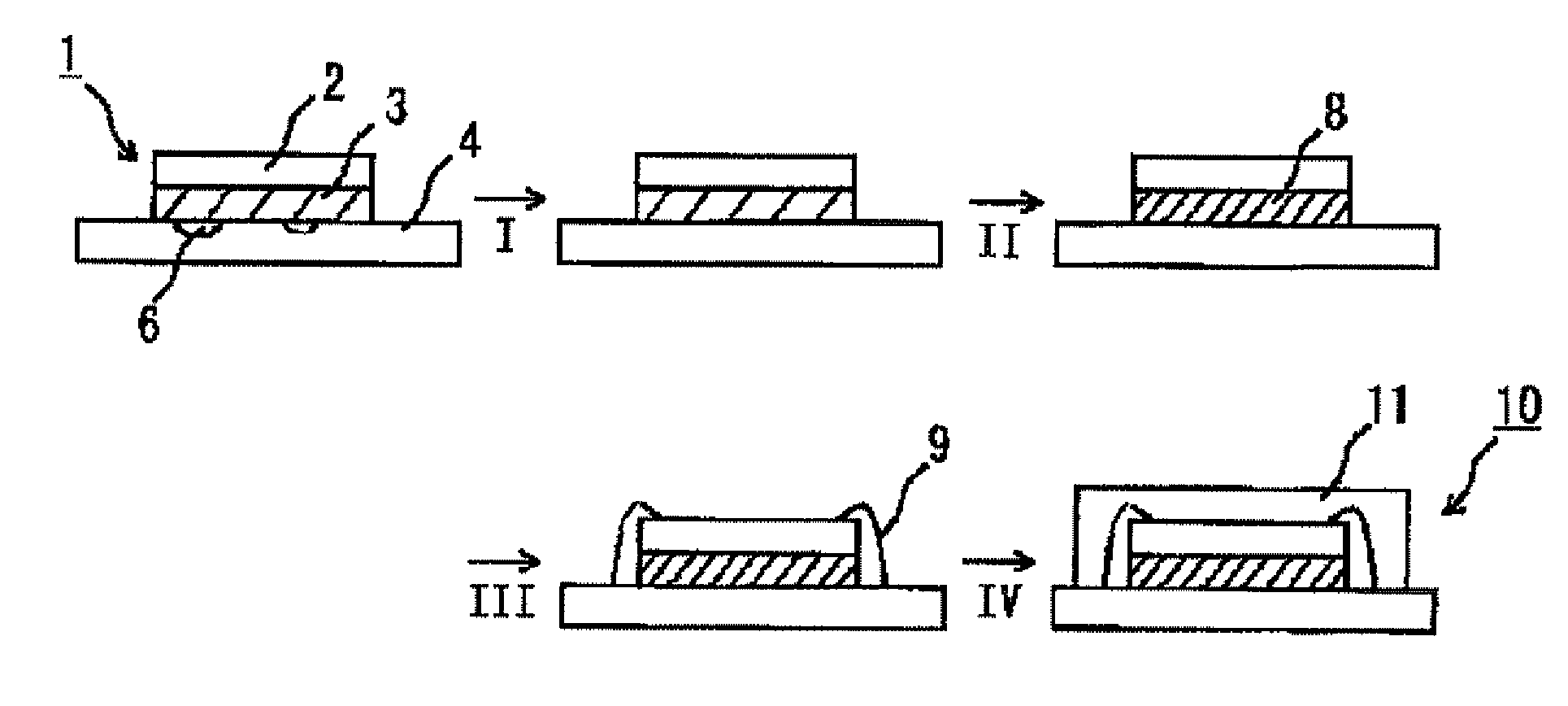
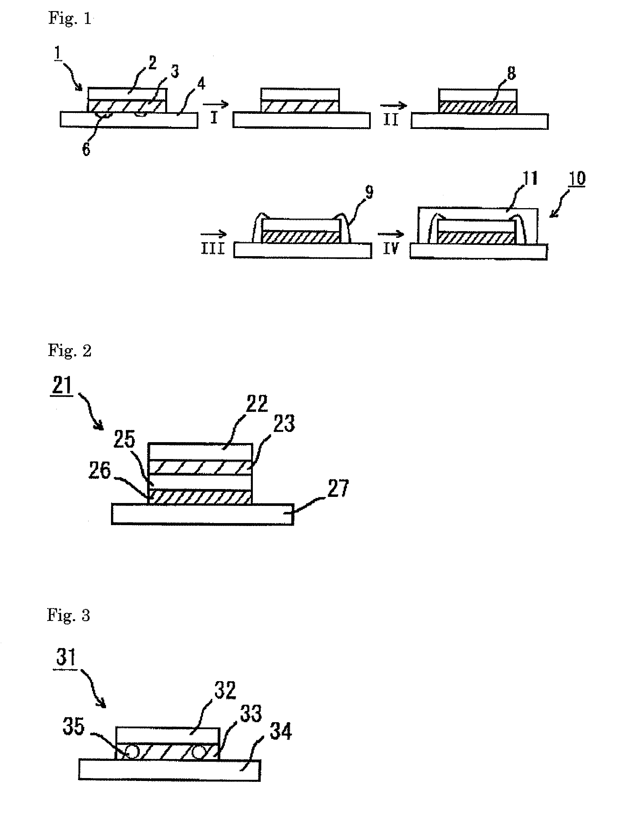
[0011] According to the process for manufacturing a semiconductor device of the present invention, a chip is mounted on a wiring board via an uncured adhesive layer under usual conditions, and voids are easily eliminated in the subsequent statically pressurizing step irrespective of the design of the wiring board. Because the pressure applied to the wiring board in the statically pressurizing step is static, the adhesive does not curl up.

Problems solved by technology

In particular, the use of a liquid adhesive frequently results in voids in the adhesive, and the use of a film adhesive often results in voids in the interface due to insufficient adhesion and insufficient followability to unevenness of an adherend surface.

Method used


Image

  • Process for manufacturing process of semiconductor device
  • Process for manufacturing process of semiconductor device
  • Process for manufacturing process of semiconductor device

Examples


example 1

(1) Dicing Step

[0082] A dicing / die-bonding sheet (Adwill LE-5003, manufactured by LINTEC Corporation) was attached to a dummy silicon wafer (200 mm in diameter, 150 μm in thickness) with use of a tape mounter (Adwill RAD 2500 m / 8, manufactured by LINTEC Corporation). The wafer was fixed to a ring frame at the same time. The dicing / die-bonding sheet was UV irradiated through a base film thereof using a UV irradiator (Adwill RAD 2000 m / 8, manufactured by LINTEC Corporation). The wafer was diced into 8 mm square chips with a dicing apparatus (DFD 651, manufactured by DISCO Corporation). The cutting depth was such that the base film of the dicing / die-bonding sheet was cut to a depth of 20 μm.

(2) Die-Bonding Step

[0083] A wiring board (manufactured by CHINO GIKEN Co,, Ltd.) used for die-bonding the chips was a copper-clad laminate (CCL-HL830, manufactured by MITSUBISHI GAS CHEMICAL COMPANY, INC.) in which the copper foil formed circuit patterns and a solder resist (PSR-4000 AUS5, man...

example 2 to example 6

[0087] Simulated semiconductor devices were manufactured in the same manner as in Example 1, except that the statically pressurizing step (3) was carried out under the conditions shown in Table 1. In Table 1, the pressure is expressed by a value by which the pressure surpassed atmospheric pressure.

TABLE 1Pressure (MPa)Temperature (° C.)Time (minutes)Ex. 10.510030Ex. 20.110030Ex. 30.910030Ex. 40.55030Ex. 50.510010Ex. 60.510060

example 7

[0088] Simulated semiconductor devices were manufactured in the same manner as in Example 1, except that the statically pressurizing step (3) and the heat curing step (4) were started and completed simultaneously. Specifically, the sticky adhesive layer was sufficiently cured at a static pressure greater than atmospheric pressure by 0.5 MPa, at 120° C. for 1 hour and then at 140° C. for 1 hour.


PUM

PropertyMeasurementUnit
Pressureaaaaaaaaaa
Pressureaaaaaaaaaa

Abstract

In a process for manufacturing a semiconductor device comprising heating a wiring board on which a chip and an uncured adhesive layer are laminated for curing the adhesive layer, the improvement includes performing a statically pressurizing step before the adhesive layer is cured, in which step the wiring board on which the chip and the uncured adhesive layer are laminated is subjected to a static pressure greater than atmospheric pressure by not less than 0.05 MPa. According to the invention, voids are easily eliminated irrespective of a design of the wiring board, and the adhesive is prevented from curling up on the chip.

Description

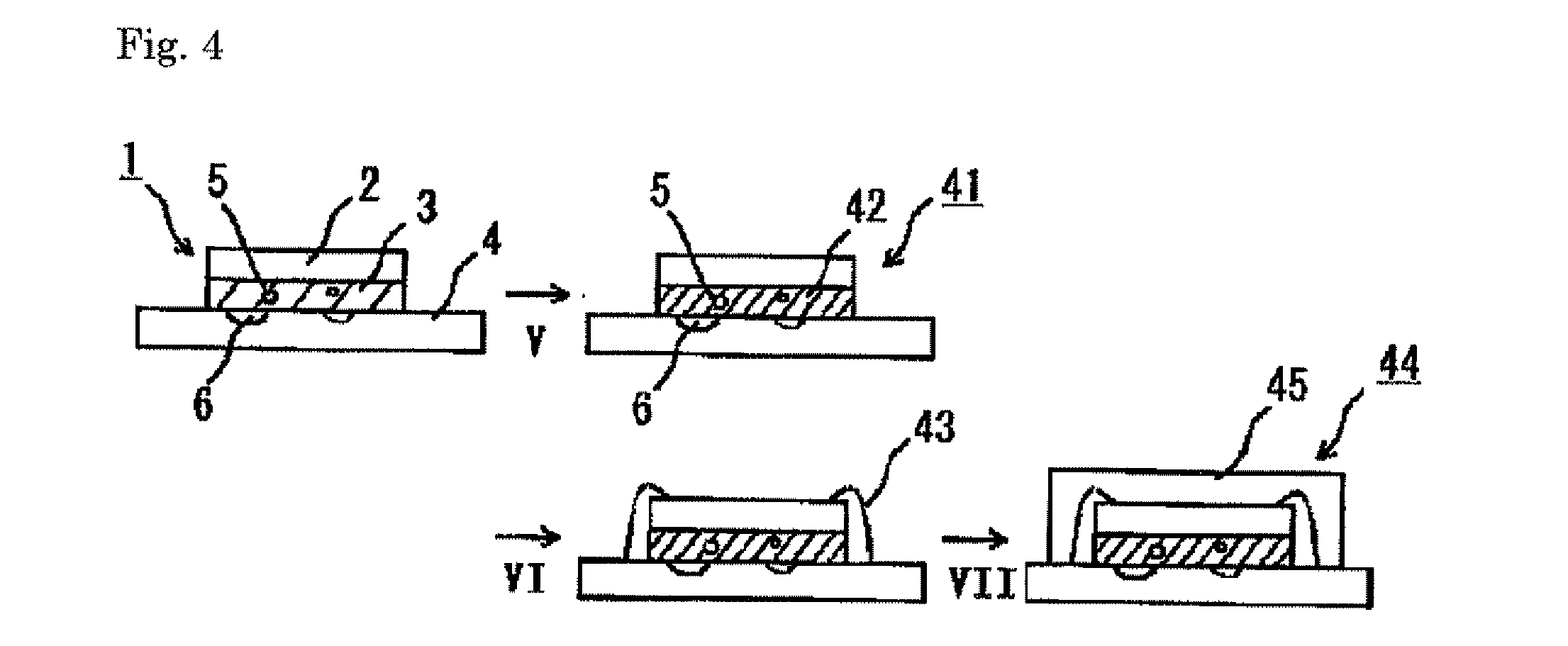
TECHNICAL FIELD [0001] The present invention relates to a process for manufacturing semiconductor devices. More particularly, the invention relates to a process for manufacturing semiconductor devices by heating a wiring board on which chips are mounted via an uncured adhesive layer to cure the adhesive layer. BACKGROUND OF THE INVENTION [0002] In conventional production of semiconductor devices, chips are die-bonded to a wiring board with a liquid thermosetting adhesive or a film thermosetting adhesive (die-bonding step), then wires are bonded (wire-bonding step), and the chips are encapsulated (encapsulating step) (FIG. 4, V to VII). When a chip 2 is mounted on a wiring board 4 via an uncured adhesive layer 3, voids 5 are often formed in the adhesive, or voids 6 may be produced in an interface between the adhesive and the chip or the wiring board (FIG. 4). Such voids do not disappear and remain after the die-bonding step (FIG. 4). In particular, the use of a liquid adhesive freque...

Claims


Application Information

Patent Timeline
IPC IPC(8): B29C65/02
CPCH01L21/6836H01L2224/32225H01L24/29H01L24/31H01L24/81H01L24/83H01L24/85H01L25/0657H01L2221/68327H01L2221/68377H01L2221/68381H01L2224/16H01L2224/27436H01L2224/2919H01L2224/29191H01L2224/48091H01L2224/73265H01L2224/81801H01L2224/83191H01L2224/83855H01L2224/92247H01L2924/01004H01L2924/01005H01L2924/01013H01L2924/01027H01L2924/01029H01L2924/01033H01L2924/01077H01L2924/01082H01L2924/07802H01L24/27H01L2924/10253H01L2224/85H01L2224/29101H01L2924/0665H01L2924/014H01L2924/01045H01L2924/01023H01L2924/01019H01L2924/01006H01L2924/00014H01L2924/0715H01L2924/0675H01L2924/069H01L2924/066H01L2924/00H01L2924/3512H01L2924/181H01L2224/73204H01L24/48H01L2924/00011H01L2924/00012H01L2224/0401H01L2224/45015H01L2924/207H01L2224/45099H01L21/50H01L21/52
Inventor YAMAZAKI, OSAMUICHIKAWA, ISAOSAIKI, NAOYA
Owner LINTEC CORP
Learn More