
Self programmable shared BIST for testing multiple memories

a self-programmable, shared technology, applied in the direction of measurement devices, functional testing, instruments, etc., can solve the problems of affecting performance, affecting the performance, and the pin count required to test a device by this method can be larger than the number of pins availabl

Inactive Publication Date: 2008-03-06
STMICROELECTRONICS PVT LTD
View PDF11 Cites 19 Cited by
  • Summary
  • Abstract
  • Description
  • Claims
  • Application Information

AI Technical Summary

Benefits of technology

"The patent describes a new on-chip testing mechanism that can test various memories on a chip using a single BIST device. This mechanism is self-programmable and can be used to test memories of different sizes and characteristics. The testing device includes a BIST controller, delay generator, interface modules, and memory wrapper. The method involves generating an initialization sequence, delaying signals, and running a test algorithm to test the memories. The technical effect of this patent is to provide a more efficient and flexible way to test multiple memories on a chip."

Problems solved by technology

However, the pin count required to test a device by this method can be larger than the number of pins available.
Also, for each memory multiplexed, additional logic will have to be introduced, which results in a slower input / output propagation time, which in turn can affect the performance.
Thus, testing embedded memories is a challenge, since testing memory cores is much more difficult than testing commodity memories due to the limitation in available pins that can be used to access the cores.
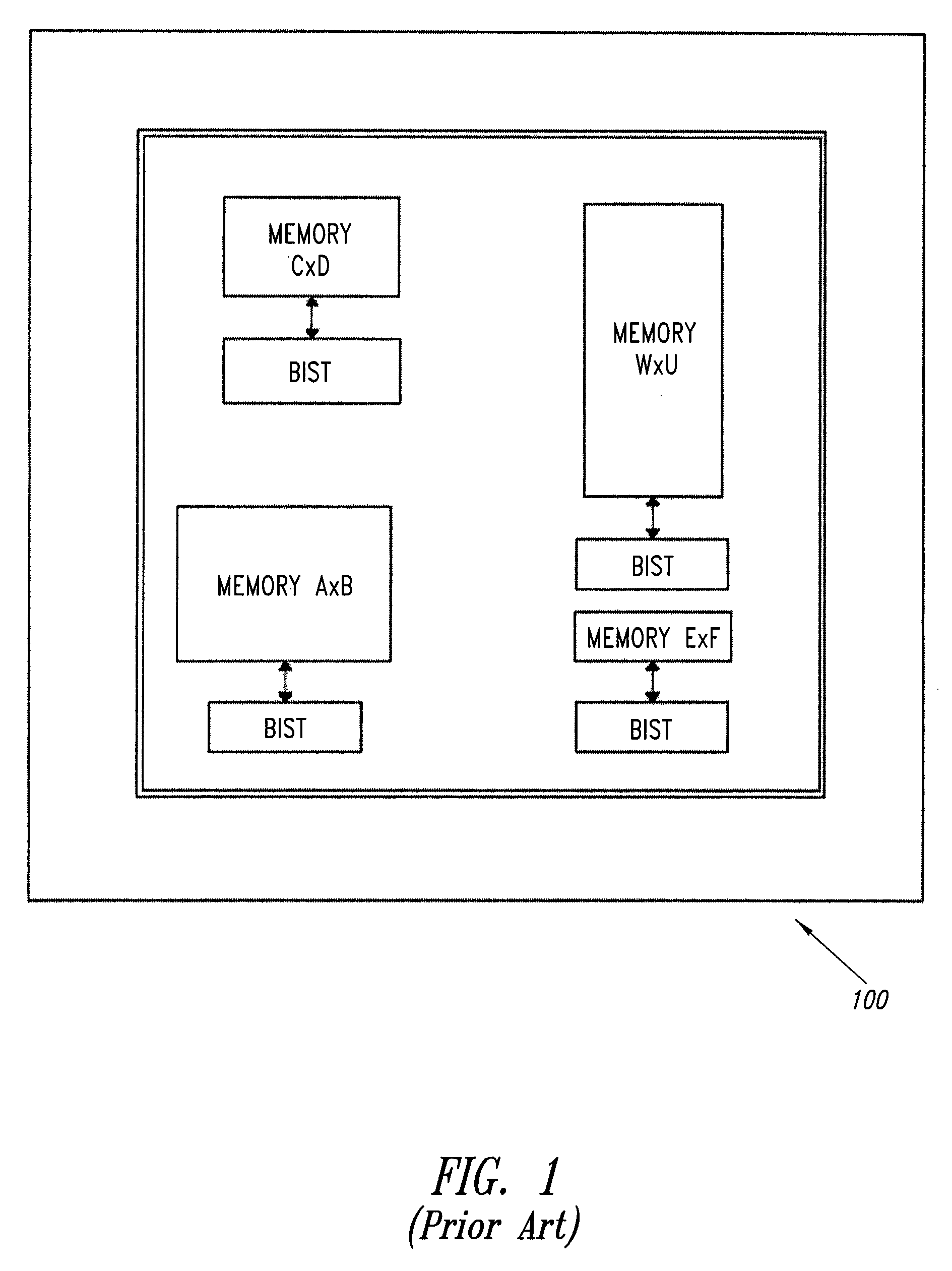
However, BIST technology consumes larger area.
The area of the BIST increases with algorithm length and complexity.
So, for a chip containing 70% of area as memory, dedicated BISTs can occupy an unacceptable amount of valuable chip area.
If the memories are working at high frequencies, then testing memories at-speed with a shared BIST becomes impossible.
The conventional methods and systems as discussed above do not overcome all the existing problems encountered in the field of chip testing like, requirement of a larger area, inability to test memories at-speed with a shared BIST, inability of a shared BIST in testing memories placed relatively far in the chip, etc.

Method used


Image

  • Self programmable shared BIST for testing multiple memories
  • Self programmable shared BIST for testing multiple memories
  • Self programmable shared BIST for testing multiple memories

Examples


Embodiment Construction

[0035] The preferred embodiments of the present invention will be described in detail with reference to the accompanying drawings. However, the present invention is not limited to the preferred embodiments. The present invention can be modified in various forms. The preferred embodiments of the present invention are only provided to explain more clearly the present invention to the ordinarily skilled in the art of the present invention. In the accompanying drawings, like reference numerals are used to indicate like components.

[0036] One embodiment provides a shared built in self testing (BIST) device for testing at-speed multiple memories, irrespective of their placement on a chip. The shared BIST is self programmable in terms of pipelined stage calculations used to test memories at-speed.

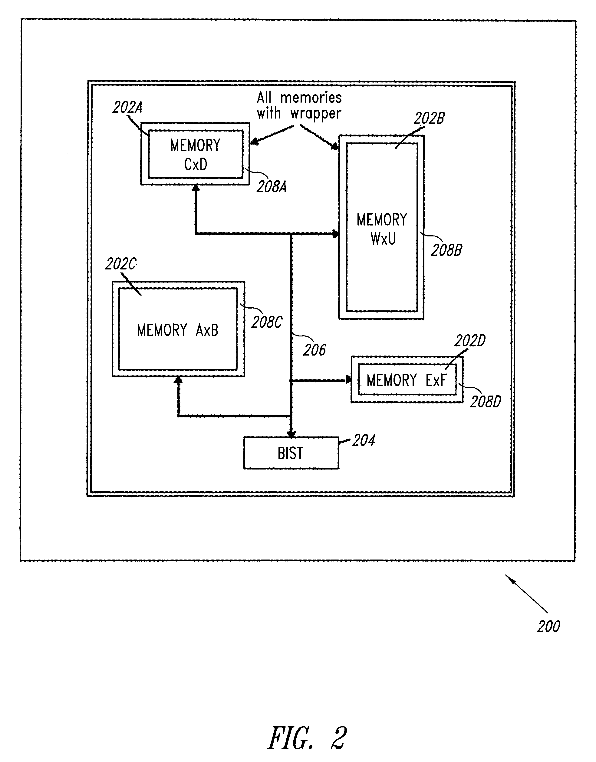
[0037]FIG. 2 illustrates a block diagram of a chip 200 having multiple memories, such as, 202A, 202B, 202C and 202D, of different size, sharing a common BIST controller 204 via a bus 206. The mem...


PUM


Abstract

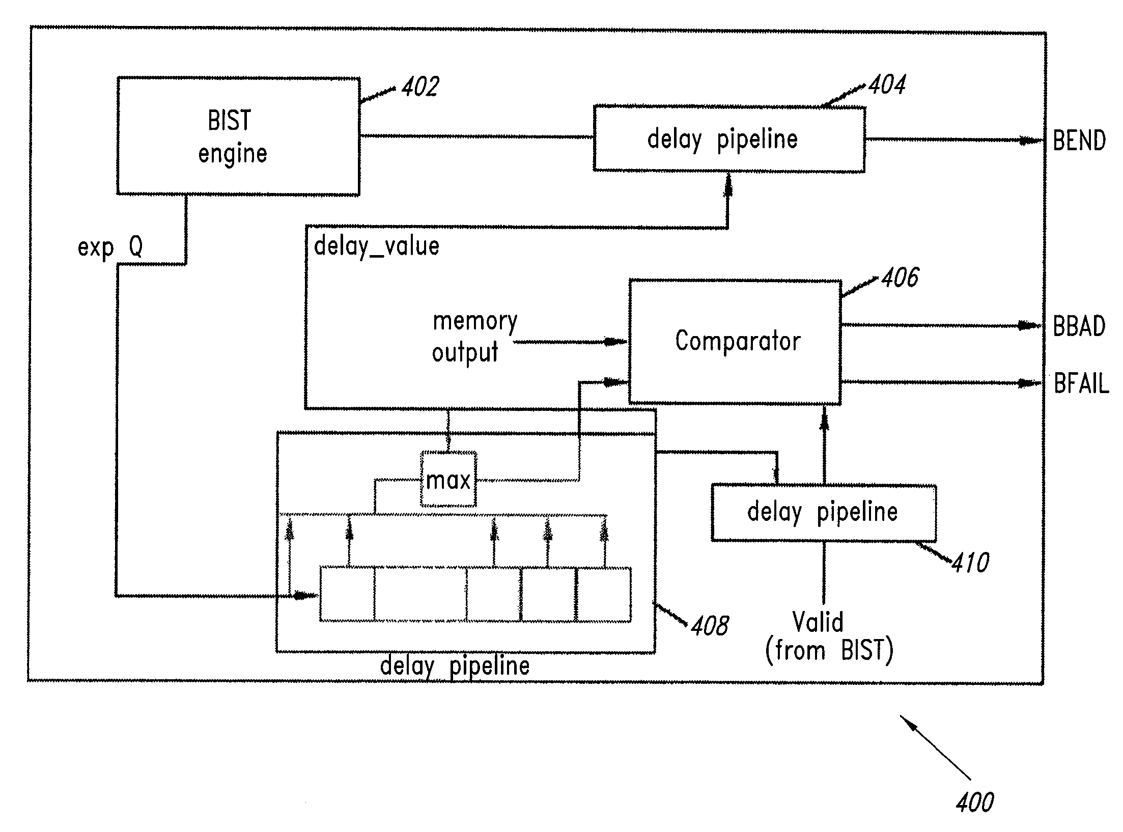
A built-in self-test (BIST) device tests multiple embedded memories of different characteristics. The BIST includes a BIST controller, a delay generator, multiple interface modules, and a memory wrapper. The BIST controller generates an initialization sequence and a memory test algorithm. The delay generator provides a delay of an expected data, a valid signal, a BBAD signal, a BEND signal, and a BFAIL signal. The multiple interface modules provide signal pipelining for multiple memories through a bus. The bus carries signals form the BIST device to multiple memories and vice-versa. The memory wrapper decodes a selected memory for decompressing a memory data signal generated by said BIST device and further compresses a memory output signal.

Description

CROSS-REFERENCE TO RELATED APPLICATION [0001] This application claims priority from Indian Patent Application No. 1948 / Del / 2006, filed on Aug. 30, 2006, which is incorporated herein by reference in its entirety. BACKGROUND [0002] 1. Technical Field [0003] The present invention relates to chip testing circuits, and more specifically to a shared built in self testing (BIST) device for testing multiple memories of various characteristics, such as various addressable sizes, various operating speeds, and various data widths. [0004] 2. Description of the Related Art [0005] Technological advancements have made it possible to integrate more and more components, even a complete system, into a single chip, called system-on-chip (SOC). Embedded memories are the most common cores in SOC design and are considered to be the vital microelectronic components of a digital logic system. [0006] Several conventional methods are available for testing integrated memory blocks. One conventional method ava...

Claims


Application Information

Patent Timeline
Patent Type & Authority Applications(United States)
IPC IPC(8): G11C29/12G06F11/27
CPCG06F11/27G11C2029/0401G11C29/16
Inventor BAHL, SWAPNIL
Owner STMICROELECTRONICS PVT LTD
Learn More