
System and Method for Mitigating Oxide Growth in a Gate Dielectric

a gate dielectric and oxide growth technology, applied in the field of gate dielectric formation with gate electrodes, can solve the problem of high transfer pressure, achieve the effects of reducing oxide growth of gate dielectric layers, improving n-incorporation uniformity, and reducing oxide growth

Active Publication Date: 2008-02-28
TEXAS INSTR INC
View PDF5 Cites 66 Cited by
  • Summary
  • Abstract
  • Description
  • Claims
  • Application Information

AI Technical Summary

Benefits of technology

The present invention relates to a method for reducing oxide growth of a gate dielectric layer during the formation of a gate dielectric structure. This method improves the uniformity of nitrogen incorporation and reduces the oxide growth of the gate dielectric, resulting in a higher nitrogen content and lower equivalent oxide thickness (EOT) of the gate dielectric. The method involves maintaining the gate dielectric in an ambient effective to mitigate oxide growth between process steps, such as an inert atmosphere or an inert gas actively purging the ambient. This results in a more stable and uniform gate dielectric structure, which can be formed across wafers and from wafer to wafer.

Problems solved by technology

This high transfer pressure, however, is offset by the need to raise and lower the pressure between each process performed in the fabrication of the gate dielectric structure.

Method used


Image

  • System and Method for Mitigating Oxide Growth in a Gate Dielectric
  • System and Method for Mitigating Oxide Growth in a Gate Dielectric
  • System and Method for Mitigating Oxide Growth in a Gate Dielectric

Examples


Embodiment Construction

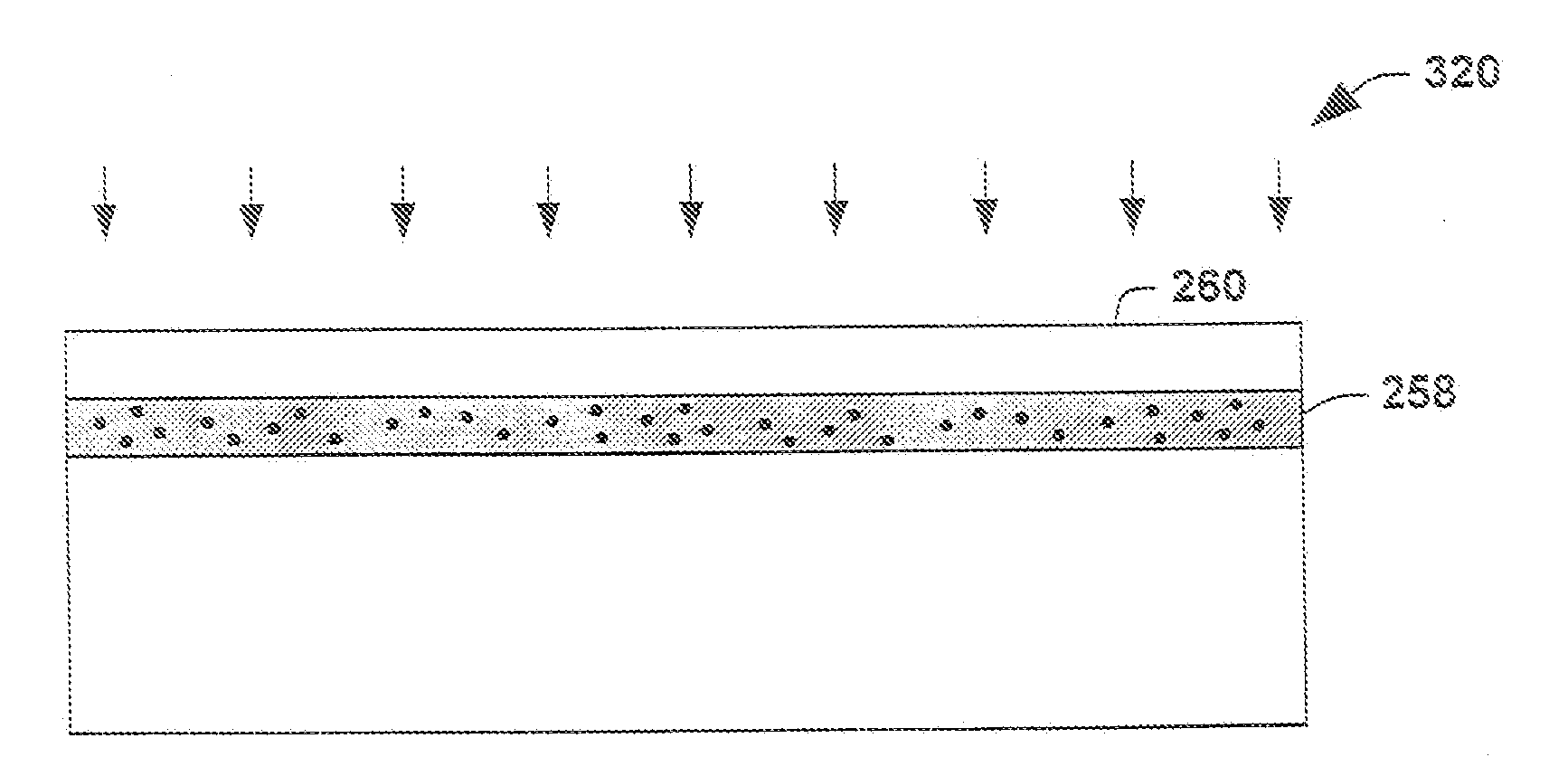
[0021] The present invention relates generally to a method of reducing oxide growth of a gate dielectric during formation of a gate dielectric structure. The reduction in oxide growth can be achieved by maintaining the gate dielectric in an ambient effective to mitigate oxide growth of the gate dielectric between at least two sequential process steps used to form the gate dielectric structure. An ambient effective to mitigate oxide growth can include an inert atmosphere that can be maintained at a pressure substantially below about 760 Torr but above vacuum (e.g., about 3 Torr to about 200 Torr). The ambient can also be actively purged with an inert gas (e.g., N2). In one aspect, a pressure of about 10 Torr to about 100 Torr (e.g., 30 Torr) can be optimum to minimize moisture and AMCs without excessively increasing the time to raise / lower the pressure to transfer the gate dielectric structure. Maintaining the pressure substantially below about 760 Torr but above vacuum, while active...


PUM

PropertyMeasurementUnit
pressuresaaaaaaaaaa
pressuresaaaaaaaaaa
pressuresaaaaaaaaaa

Abstract

Oxide growth of a gate dielectric layer that occurs between processes used in the fabrication of a gate dielectric structure can be reduced. The reduction in oxide growth can be achieved by maintaining the gate dielectric layer in an ambient effective to mitigate oxide growth of the gate dielectric layer between at least two sequential process steps used in the fabrication the gate dielectric structure. Maintaining the gate dielectric layer in an ambient effective to mitigate oxide growth also improves the uniformity of nitrogen implanted in the gate dielectric.

Description

[0001] This application is a continuation of Ser. No. 11 / 145,674 filed Jun. 6, 2005 which is a divisional of application Ser. No. 10 / 436,848, filed May 13, 2003, now U.S. Pat. No. 6,921,703.TECHNICAL FIELD [0002] The present invention relates to processes for the manufacture of semiconductor devices and, more particularly, to the formation of a gate dielectric with a gate electrode. BACKGROUND OF THE INVENTION [0003] In complementary metal oxide silicon (CMOS) technology, a need to enhance the speed and increase the density of CMOS integrated circuits (IC's) has resulted in the evolution of transistor scaling, accompanied by progressively thinner gate dielectric oxide. Reduction in the thickness of a gate dielectric provides increased drive current, with resultant increased speed. In addition, a thinner gate dielectric offers enhanced control of channel charge, thereby reducing short channel effects. The fabrication of thinner gate oxides, however, presents gate leakage current and ...

Claims


Application Information

Patent Timeline
Patent Type & Authority Applications(United States)
IPC IPC(8): H01L21/336H01L21/4763
CPCH01L21/28167H01L21/28194H01L21/28202H01L21/31604H01L29/78H01L29/4908H01L29/513H01L29/517H01L29/518H01L21/318H01J37/32752H01J37/32825H01J37/32899H01L21/02323H01L21/02181H01L21/02318H01L21/02326H01L21/0223H01L21/02255H01L21/0228H01L21/02252H01L21/02329H01L21/28035H01L21/28185H01L21/67161H01L21/67201H01L21/02332H01L21/28229H01L21/3105H01L21/3205H01L21/6776H01L21/324H01L29/42364H01L29/4916H01L29/66477H01L21/0234H01L21/67167H01L21/67196C23C16/45557C23C16/4582H01J2237/3321H01L21/28158
Inventor BEVAN, MALCOLM J.BU, HAOWENNIIMI, HIROAKIALSHAREEF, HUSAM N.
Owner TEXAS INSTR INC
Learn More