Semiconductor package, method of production thereof and encapsulation resin
a technology of semiconductors and encapsulation resins, applied in semiconductor devices, solid-state devices, basic electric elements, etc., can solve problems such as inability to reliably prevent cracks, damage to chips, and conventional solutions, and achieve the effects of preventing or reducing cracks, and high reliability
- Summary
- Abstract
- Description
- Claims
- Application Information
AI Technical Summary
Benefits of technology
Problems solved by technology
Method used
Image

Examples
examples
[0183]Herebelow, examples of the present invention shall be described, but the present invention is not to be construed as being limited thereto.
1. Test of Physical Properties of Cured Resin
[0184]Encapsulation resin compositions 1-6 were prepared. Table 1 shows the compositions of the encapsulation resin compositions and the results of measurements of glass transition temperature, coefficient of thermal expansion, flexural modulus and viscosity.
[0185]With regard to the glass transition temperature, after the encapsulation resin compositions were cured at 150° C.×120 minutes, they were cut into 5×5×10 mm samples, and these samples were measured using a Seiko TMA / SS120 with a press load of 5 g, in the temperature range of −100° C. to 300° C. at a temperature increase of 10° C. / minute. The coefficient of thermal expansion was also obtained by the same measurement. As for the flexural modulus, the encapsulation resin compositions were formed into pieces of width 10 mm, length about 150 ...
examples 1-6
(2) Examples 1-6 of Present Invention
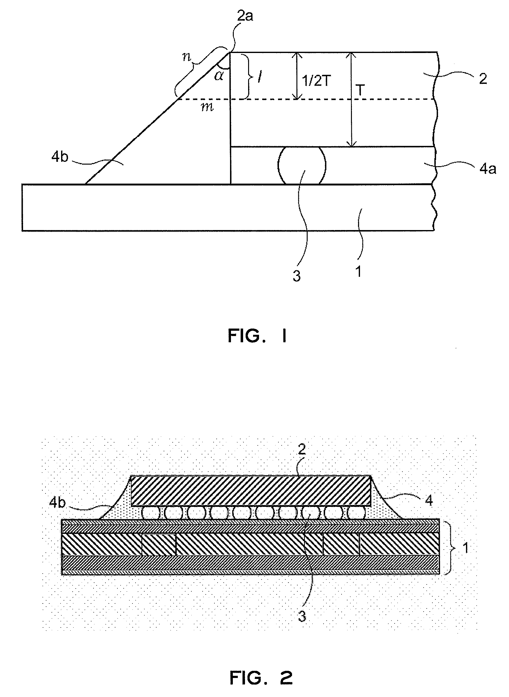
Fillet Size Small Inclination Angle 50° or Less
[0196]Conditions: Samples were subjected to a pretreatment at 30° C., 60%, 168 hours, reflow resistance test (peak temperature 260° C., three times)+thermal cycling test (500 cycles at −55° C. (30 minutes) / 125° C. (30 minutes)), then inspected for cracks. The number of defective semiconductor packages having cracks with respect to the total number of samples is indicated by “defects / total samples”. The test results are shown in Table 5.
TABLE 5EX1EX2EX3EX4EX5EX6CircuitCore LayerCore LayerInsulationEncapsulation Resin TypeBoardTypeThicknessLayer TypeER1ER2ER3ER4ER5ER6CB A679FG0.4 mmtABF-GX130 / 30 / 30 / 30 / 30 / 30 / 3CB B679FG0.2 mmtABF-GX130 / 20 / 20 / 20 / 20 / 20 / 2CB CELC4785GS0.4 mmtAPL36010 / 30 / 30 / 30 / 30 / 30 / 3CB DELC4785GS0.2 mmtAPL36010 / 20 / 20 / 20 / 20 / 20 / 2CB EELC4785GS0.2 mmtAPL36510 / 30 / 30 / 30 / 30 / 30 / 3CB F679FG0.4 mmtAPL36010 / 30 / 30 / 30 / 30 / 30 / 3
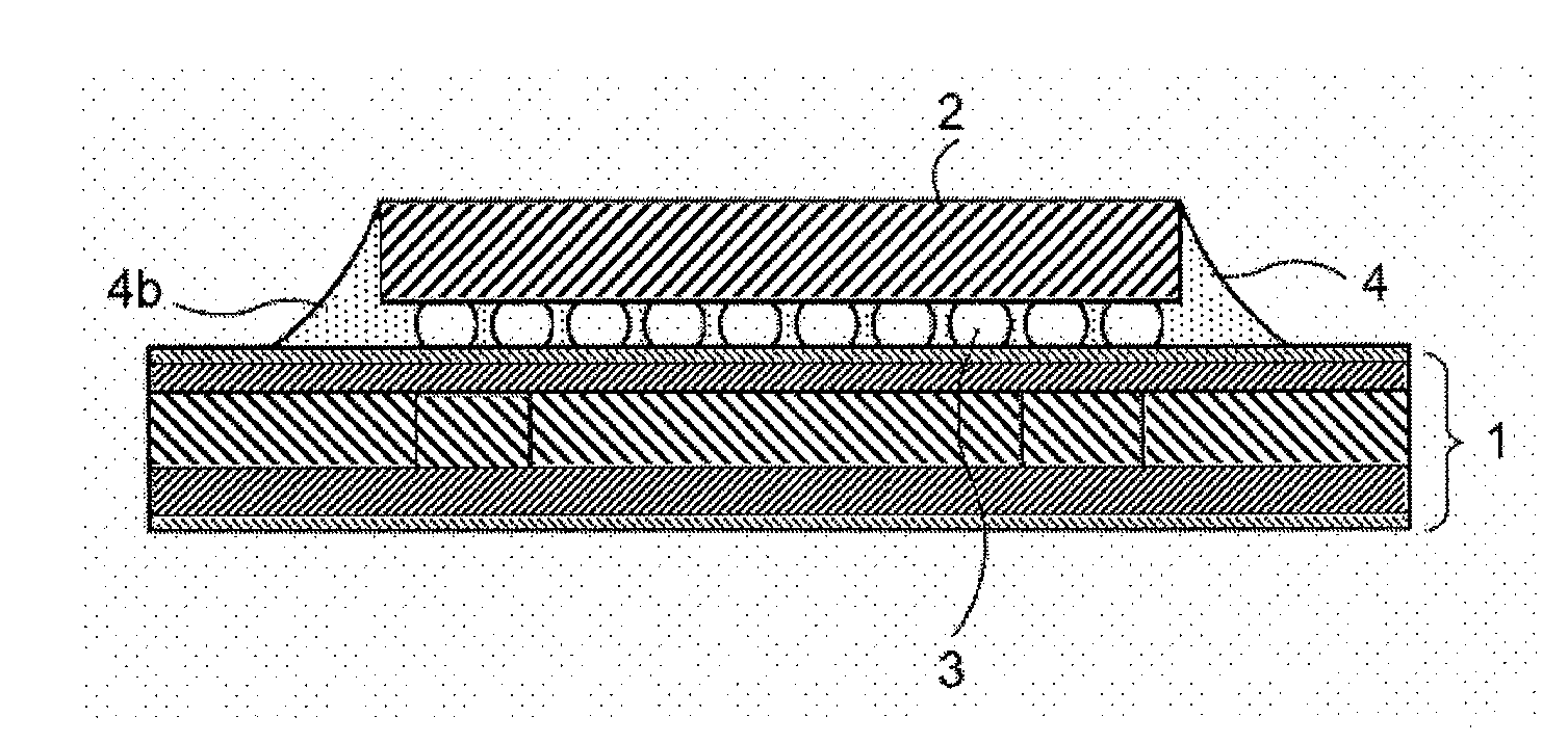
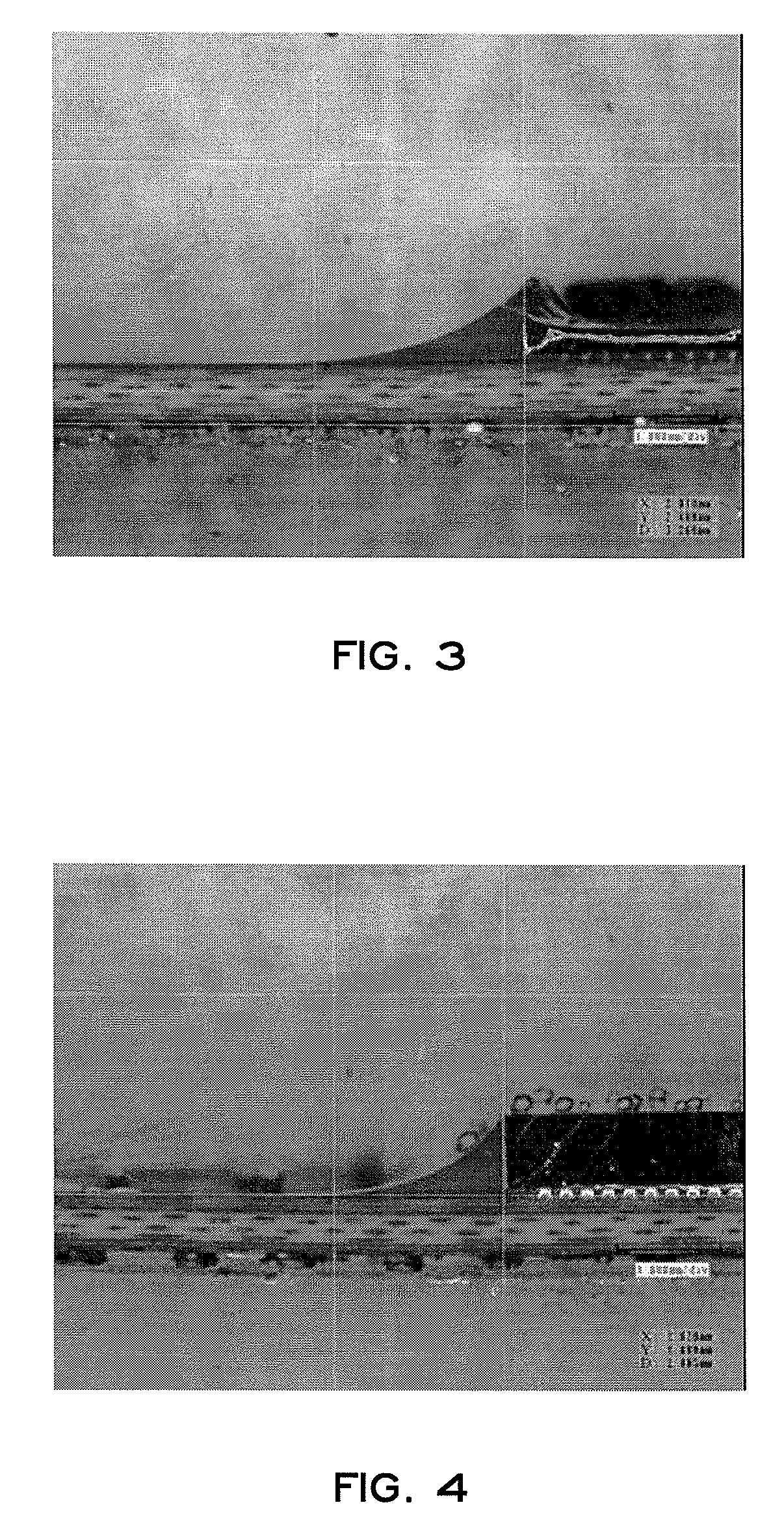
3. Observation of Shape of Fillet
[0197]FIG. 3 is a photograph of a cross section ...
PUM
| Property | Measurement | Unit |
|---|---|---|
| angle | aaaaa | aaaaa |
| angle | aaaaa | aaaaa |
| glass transition temperature | aaaaa | aaaaa |
Abstract
Description
Claims
Application Information
 - R&D
- Intellectual Property
- Life Sciences
- Materials
- Tech Scout
- Unparalleled Data Quality
- Higher Quality Content
- 60% Fewer Hallucinations
Browse by: Latest US Patents, China's latest patents, Technical Efficacy Thesaurus, Application Domain, Technology Topic, Popular Technical Reports.
© 2025 PatSnap. All rights reserved.Legal|Privacy policy|Modern Slavery Act Transparency Statement|Sitemap|About US| Contact US: help@patsnap.com