Optimization Of Geometry Pattern Density

a geometry pattern and density technology, applied in the field of optimization of geometry pattern density, can solve the problems of loss of contact, uneven next layer, variety of circuit structure flaws, etc., and achieve the effect of maximizing the area of the fill region and reducing the number of fill polygons

Inactive Publication Date: 2008-02-07
MENTOR GRAPHICS CORP
View PDF3 Cites 18 Cited by
  • Summary
  • Abstract
  • Description
  • Claims
  • Application Information

AI Technical Summary

Benefits of technology

[0010] Advantageously, various examples of the invention provide techniques for optimizing the pattern density in the circuit layout design of a circuit layer. According to various implementations of the invention, a layer in circuit design is analyzed to define empty regions that can be filled with fill polygons (referred to hereafter as “fill” regions). With some examples of the invention, a designer or manufacturer may specify constraints for defining the fill regions, so that fill polygons cannot inadvertently be placed too closely to functional polygons. Next, a pattern of fill

Problems solved by technology

One problem with conventional planarization methods is that different materials will have different densities, so softer materials will be polished more than harder materials.
As a result, a layer's surface may become uneven, causing the next layer to be more uneven.
Such irregular surface topographies may cause a variety of flaws in the circuit structures, such as holes, loss of contact, and other manufacturing defects.
While this corrective technique usually improves the planarity of layers in an integrated circuit, it has some drawbacks.
This process can be very time consuming and tedious.
Moreover, adding fill polygons may increase the capacitance of the lay

Method used


Image

  • Optimization Of Geometry Pattern Density
  • Optimization Of Geometry Pattern Density
  • Optimization Of Geometry Pattern Density

Examples


Embodiment Construction

Operating Environment

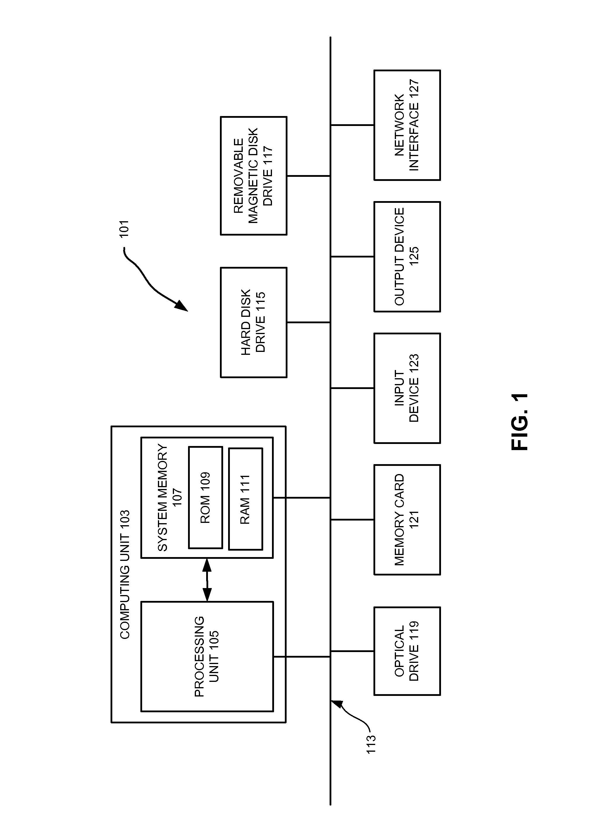
[0022] Various examples of the invention may be implemented through the execution of software instructions by a computing device, such as a programmable computer. Accordingly, FIG. 1 shows an illustrative example of a computing device 101. As seen in this figure, the computing device 101 includes a computing unit 103 with a processing unit 105 and a system memory 107. The processing unit 105 may be any type of programmable electronic device for executing software instructions, but will conventionally be a microprocessor. The system memory 107 may include both a read-only memory (ROM) 109 and a random access memory (RAM) 111. As will be appreciated by those of ordinary skill in the art, both the read-only memory (ROM) 109 and the random access memory (RAM) 111 may store software instructions for execution by the processing unit 105.

[0023] The processing unit 105 and the system memory 107 are connected, either directly or indirectly, through a bus 113 or altern...


PUM


Abstract

Techniques are provided for optimizing the pattern density in the circuit layout design of a circuit layer. A layer in circuit design is analyzed to define fill regions that can be filled with fill polygons A pattern of fill polygons also is generated, to fill the fill regions. The layout design for the layer then is divided into separate areas or “windows,” and a target density for each window is determined. More particularly, each window is analyzed to determine a target density for the window that will satisfy specified density constraint values, such as a minimum density constraint, a maximum density constraint, or a maximum density gradient constraint. In some implementations, the target density will be the smallest density that will comply with each of the specified density value constraints. Once the target density for the window has been determined, the fill polygons required to most closely approach this target density are selected and added to the circuit layout design. With some implementations, this process may be repeated for fill polygons of different sizes or shapes.

Description

RELATED APPLICATIONS [0001] This application claims priority under 35 U.S.C. §119 to U.S. Provisional Patent Application No. 60 / 853,309 entitled “Optimization Of Pattern Density,” filed on May 1, 2006, naming Eugene Anikin as inventor, and originally assigned U.S. patent application Ser. No. 11 / 415,878, which application is incorporated entirely herein by reference.FIELD OF THE INVENTION [0002] The present invention relates to various techniques and tools to assist in the design of circuits, such as integrated circuits. Various aspects of the present invention are particularly applicable to optimizing the pattern density of a layer of a circuit. BACKGROUND OF THE INVENTION [0003] Electronic circuits, such as integrated microcircuits, are used in a variety of products, from automobiles to microwaves to personal computers. Designing and fabricating microcircuit devices typically involves many steps, known as a “design flow.” The particular steps of a design flow are highly dependent u...

Claims


Application Information

Patent Timeline
IPC IPC(8): G06F17/50
CPCG06F2217/12G06F17/5068G06F30/39G06F2119/18Y02P90/02
Inventor ANIKIN, EUGENEPIKUS, FEDOR G.STEDMAN, JOHN W.GRODD, LAURENCEABERCROMBIE, DAVID
Owner MENTOR GRAPHICS CORP
Why Eureka
Try Eureka