Apparatus and method for a singulation of polymer waveguides using photolithography

a technology of polymer waveguides and photolithography, applied in the field of polymer waveguides, can solve the problems of reducing the life of the battery in the device, obscuring the viewing of the underlying display, and dim display

Inactive Publication Date: 2008-02-07
POA SANA LIQUIDATING TRUST
View PDF48 Cites 16 Cited by
  • Summary
  • Abstract
  • Description
  • Claims
  • Application Information

AI Technical Summary

Problems solved by technology

This approach has a number of problems.
Foremost, the film causes the display to appear dim and obscures viewing of the underlying display.
However, in the case of most portable devices, such as cell phones, personal digital assistants, and laptop computers, the added intensity requires additional power, reducing the life of the battery in the device.
The films are also easily damaged.
In addition, the cost of the film scales dramatically with the size of the screen.
With large screens, the cost is typically prohibitive.
This type of data input display, however, also has a number of problems.
The relatively large number of LEDs and photodiodes, and the need for precise alignment, make such displays complex, expensive, and difficult to manufacture.
Singulation is a problem with the aforementioned polymer waveguides.
The problem with using a dicing saw is that a high degree of precision and smoothness is required, particularly at points where the waveguide lenses are located or where the waveguide will be coupled to an optical sensitive device (e.g., a CCD) or a light transmitting device (e.g., a laser, LED or LCD).
If the cuts are not clean and precise, light may scatter, adversely effecting the operation of the waveguide.
Use of dicing saw is also very expensive as the waveguides need to be individually cut.
The time and equipment needed to singulate a large number of waveguides is therefore very costly.
Furthermore, if the cuts are not precise enough, yields of the waveguides may be reduced, further increasing costs.

Method used


Image

  • Apparatus and method for a singulation of polymer waveguides using photolithography
  • Apparatus and method for a singulation of polymer waveguides using photolithography
  • Apparatus and method for a singulation of polymer waveguides using photolithography

Examples


Embodiment Construction

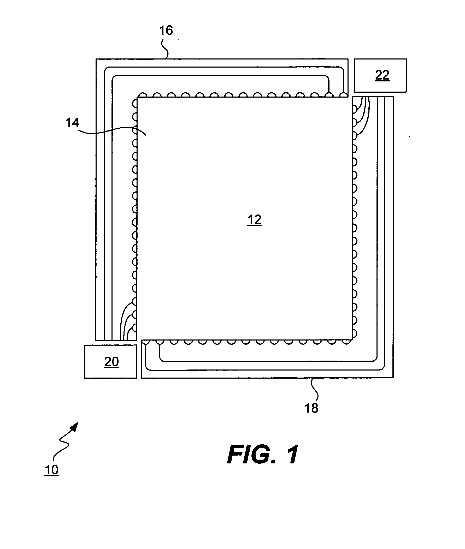
[0019]Referring to FIG. 1, a touch screen data input device is shown. The data input device 10 defines either a grid or “lamina”12 of light in the free space adjacent to a touch screen 14. The grid or lamina 12 of light is created by an X and Y input light polymer waveguide 16. An opposing receives X and Y polymer waveguide 18 is provided to detect data entries to the input device by determining the location of interrupts in the grid or lamina 12 caused when data is entered to the input device. A light source 20, such as a laser or LCD, is optically coupled to the transmit waveguide 16. An optical processor 22 is coupled to the receive waveguide 18. During operation, a user makes a data entry to the device 10 by touching the screen 14 using an input device, such as a finger, pen or stylus. During the act of touching the screen, the grid or lamina 12 of light in the free space adjacent the screen is interrupted. The optical processor 22 detects the X and Y coordinates of the interrup...


PUM


Abstract

Singulating polymer waveguides made on a substrate using photolithography. A first polymer cladding layer is formed and patterned on a first surface of a substrate to form a plurality of bottom cladding elements. Each of the bottom cladding elements are structurally independent from the other bottom cladding elements on the substrate. A second polymer layer is then formed and patterned on each of the bottom cladding elements to form a plurality of waveguide cores on each of the plurality of bottom cladding elements respectively. A third polymer top cladding layer is next formed over the plurality of waveguide cores on each of the bottom cladding elements respectively. In various embodiments, the individual waveguides can be separated from the substrate by using a selective tape or by cutting or sawing the substrate between the bottom cladding elements. The bottom cladding elements, the plurality of waveguide cores formed from the patterned second polymer layer, and the top cladding layer forming a plurality of polymer waveguides on the substrate.

Description

BACKGROUND OF THE INVENTION[0001]1. Field of the Invention[0002]The present invention relates generally to polymer waveguides used for light generation and reception in touch screen displays, and more particularly, to singulating polymer waveguides made on a substrate using photolithography.[0003]2. Description of the Related Art[0004]User input devices for data processing systems can take many forms. Two types of relevance are touch screens and pen-based screens. With either a touch screen or a pen-based screen, a user may input data by touching the display screen with either a finger or an input device such as a stylus or pen.[0005]One conventional approach to providing a touch or pen-based input system is to overlay a resistive or capacitive film over the display screen. This approach has a number of problems. Foremost, the film causes the display to appear dim and obscures viewing of the underlying display. To compensate, the intensity of the display screen is often increased. H...

Claims


Application Information

Patent Timeline
IPC IPC(8): G02B6/10B29D11/00
CPCG02B6/1221G02B2006/12069G02B6/138G02B6/136
Inventor PAYNE, JONATHAN
Owner POA SANA LIQUIDATING TRUST
Why Eureka
Try Eureka