
Structure of image sensor module and a method for manufacturing of wafer level package

a technology of image sensor module and manufacturing method, which is applied in the direction of electrical equipment, semiconductor devices, radio frequency control devices, etc., can solve the problems of reducing yield, reducing the yield, and reducing the yield of frame package technology, so as to facilitate the final testing of wafer level packages, reduce the cost of package structure, and increase the yield of package structure

Inactive Publication Date: 2008-01-24
ADVANCED CHIP ENG TECH
View PDF42 Cites 18 Cited by
  • Summary
  • Abstract
  • Description
  • Claims
  • Application Information

AI Technical Summary

Benefits of technology

[0011]Another objective of the present invention is to provide an image sensor module to conveniently make a final testing of the wafer level package.
[0012]Still objective of the present invention is to lower the cost of the package structure.
[0013]Still another objective of the present invention is to raise the yield of the package structure.
[0014]Still another objective of the present invention is to offer the thinner body of the image sensor package and module.
[0015]Another objective of the present invention is to provide package structure with a high yield and reliability, and it can apply for semiconductor industry and LCD industry.

Problems solved by technology

It causes the packaging for the semiconductor dice to become more difficult and decrease the yield.
The earlier lead frame package technology is already not suitable for the advanced semiconductor dice due to the density of the pins thereof is too high.
The one drawback of the method of the COB is lower yield rate during packaging process due to particle contamination on sensing area.
Besides, the drawbacks of the method of the LCC are higher packaging cost due to materials and lower yield rate during packaging process due to particle contamination on sensing area.
Moreover, SHELL CASE company also develops wafer level package technique, the image sensor dice packaged by the SHELL CASE is higher cost due to requiring two glass plate and complicate process.
And, the transparency is bad due to epoxy wearing out, and the potential reliability may be reduced.

Method used


Image

  • Structure of image sensor module and a method for manufacturing of wafer level package
  • Structure of image sensor module and a method for manufacturing of wafer level package
  • Structure of image sensor module and a method for manufacturing of wafer level package

Examples


Embodiment Construction

[0026]Some sample embodiments of the invention will now be described in greater detail. Nevertheless, it should be recognized that the present invention can be practiced in a wide range of other embodiments besides those explicitly described, and the scope of the present invention is expressly not limited expect as specified in the accompanying claims.

[0027]Then, the components of the different elements are not shown to scale. Some dimensions of the related components are exaggerated and meaningless portions are not drawn to provide a more clear description and comprehension of the present invention.

[0028]The die of the present invention may be packaged with passive components (ex. capacitors) or other dice with a side by side structure or a stacking structure. The IC package can be finished by semiconductor industry and LCD, PCB industry.

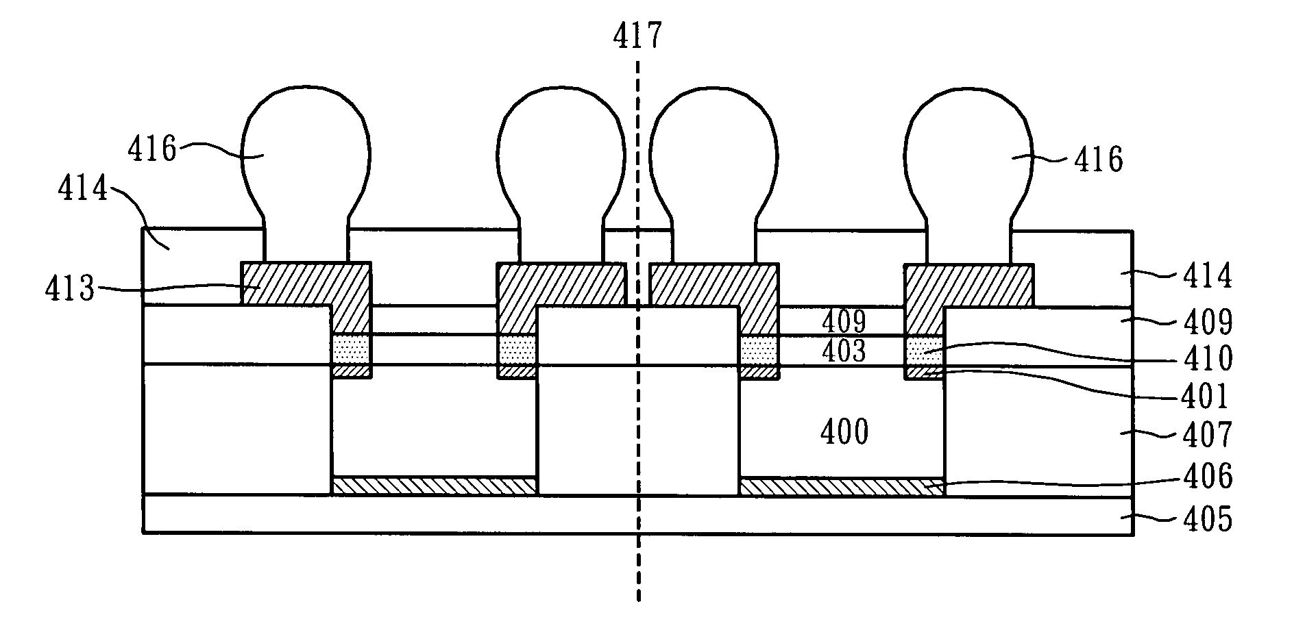
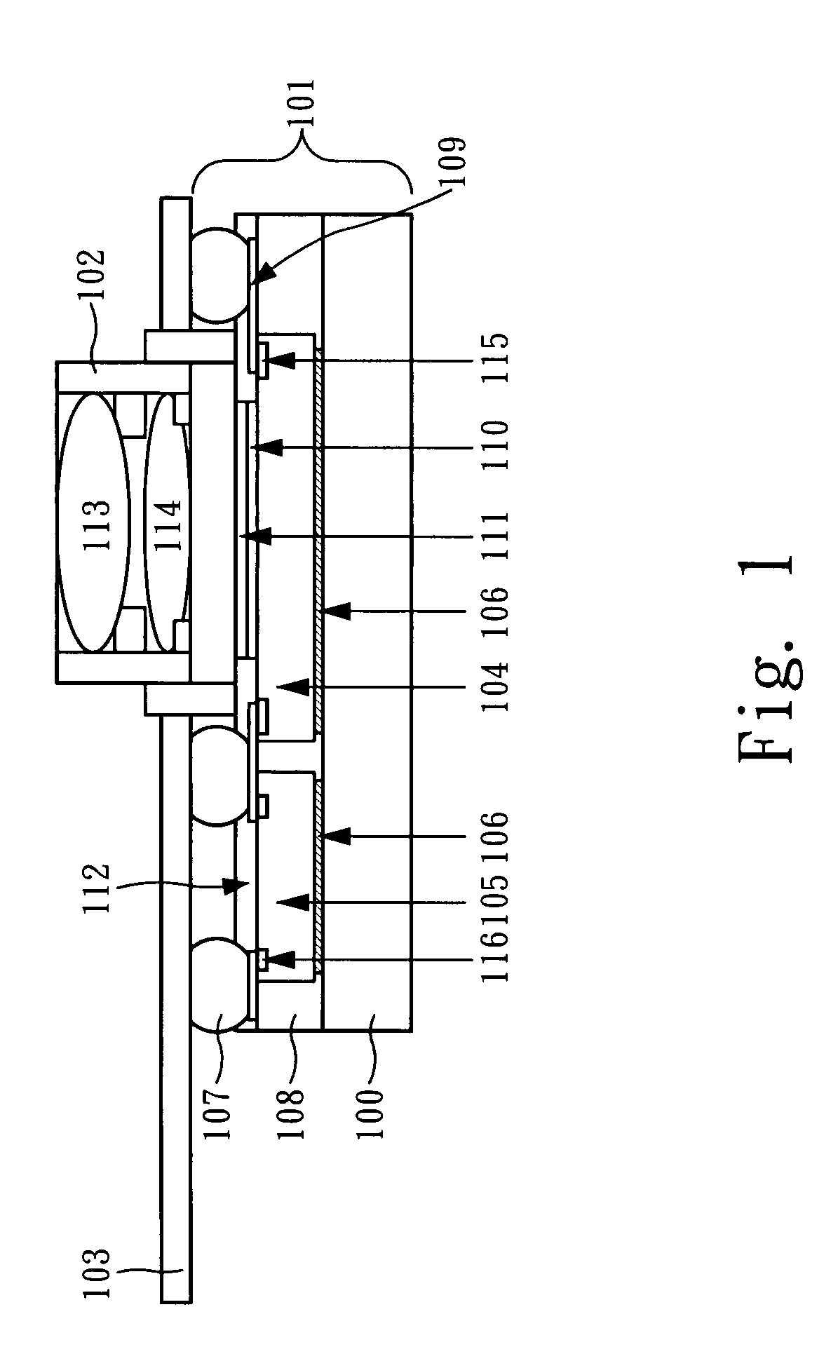
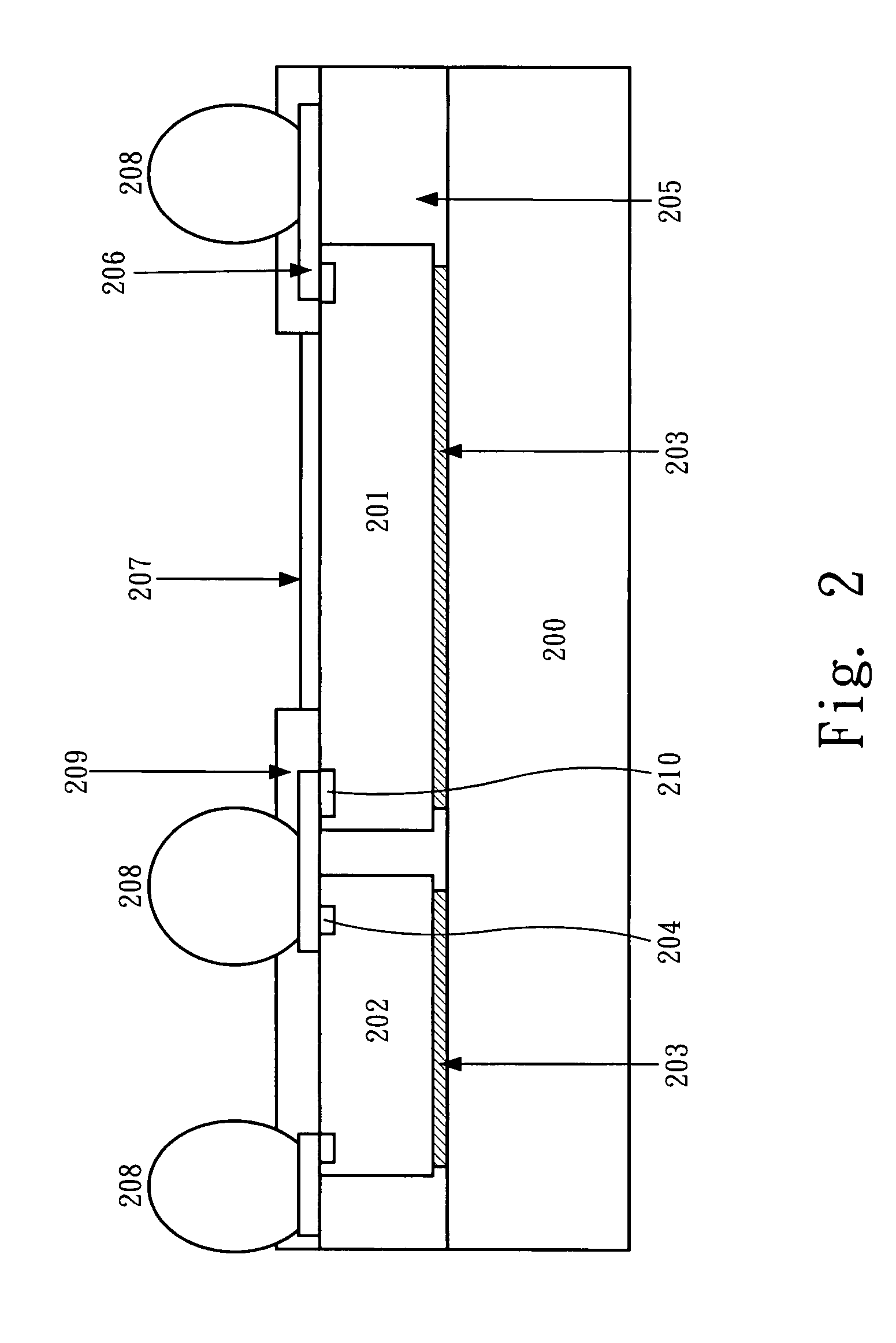
[0029]As aforementioned, the present invention provides an image sensor module, as shown in FIG. 1. The cross-section of the wafer level package s...


PUM


Abstract

The present invention discloses an image sensor module and forming method of wafer level package. The image sensor module comprises a metal alloy base, a wafer level package, a lens holder, and flexible printed circuits (F.P.C.). The wafer level package having a plurality of image sensor dice and a plurality of solder balls is attached to the metal alloy base. A plurality of lens are placed in the lens holder, and the lens holder is located on the image sensor dice. The lens holder is placed in the flexible printed circuits (F.P.C.), and the flexible printed circuits (F.P.C.) has a plurality of solder joints coupled to the solder balls for conveniently transmitting signal of the image sensor dice. Moreover, the image sensor dice may be packaged with passive components or other dice with a side by side structure or a stacking structure.

Description

CROSS-REFERENCE TO RELATED APPLICATION[0001]This is a divisional application of the application of Ser. No. 11 / 488,653, filed on Jul. 19, 2006, now pending, of which the entire disclosure is hereby incorporated by reference.BACKGROUND OF THE INVENTION[0002]1. Field of the Invention[0003]This invention relates to an image sensor module, and more particularly to an image sensor module and a structure and method for manufacturing of wafer level package that can lower the cost, raise the yield and reliability.[0004]2. Description of the Prior Art[0005]The semiconductor technologies are developing very fast, and especially semiconductor dice have a tendency toward miniaturization. However, the requirements for the functions of the semiconductor dice have an opposite tendency to variety. Namely, the semiconductor dice must have more I / O pads into a smaller area, so the density of the pins is raised quickly. It causes the packaging for the semiconductor dice to become more difficult and de...

Claims


Application Information

Patent Timeline
Patent Type & Authority Applications(United States)
IPC IPC(8): H01L21/00
CPCH01L24/19H01L2924/01075H01L27/14625H01L27/14632H01L27/14685H01L27/14687H01L2224/24226H01L2924/01013H01L2924/01029H01L2924/01033H01L2924/01077H01L2924/01078H01L2924/01079H01L2924/01082H01L2924/01006H01L2924/01024H01L2924/01047H01L2924/01074H01L27/14618H01L2924/15787H01L24/97H01L2224/12105H01L2224/24137H01L2224/73267H01L2224/97H01L2924/14H01L2224/05026H01L2224/05548H01L2224/05023H01L2224/05001H01L2224/05147H01L2224/05166H01L2224/05644H01L2224/05647H01L2224/05655H01L2224/94H01L2224/32145H01L2224/32245H01L24/05H01L2224/02379H01L2924/00H01L2224/83H01L2224/82H01L2924/00014H01L2224/214H01L27/146
Inventor YANG, WEN-KUNYANG, WEN PIN
Owner ADVANCED CHIP ENG TECH
Learn More