Semiconductor device

Inactive Publication Date: 2008-01-10
SOCIONEXT INC
View PDF7 Cites 1 Cited by
  • Summary
  • Abstract
  • Description
  • Claims
  • Application Information

AI Technical Summary

Benefits of technology

[0007]An object of the present invention is minimizing the circuit scale of a circuit for testing an A / D conversion circuit.
[0009]With the above configuration, since the conversion results from the A / D conversion circuit are not stored every time the conversion result is updated, the circuit scale can be suppressed, and yet the computation result can be obtained based on a plurality of conversion results. The circuit scale does not change so largely with increase in the number of A / D conversion results used for computation. Thus, the computation can be made based on a larger number of A / D conversion results, and this can suppress the influence of noise.
[0010]According to the present invention, a noise component affecting the A / D conversion result can be removed while the circuit scale is suppressed. It is therefore easily possible to test the A / D conversion circuit correctly.

Problems solved by technology

However, if the influence of noise caused by electromagnetic waves originating from a testing device (LSI tester), a substrate for testing and surrounding facilities becomes great during the testing, the A / D conversion accuracy may degrade, resulting in failure to perform appropriate testing.
For this reason, noise of minute voltages that would have conventionally caused no problem has become a major cause for reducing the A / D conversion accuracy.
However, the noise removal technology described above has the following problems.

Method used


Image

  • Semiconductor device
  • Semiconductor device
  • Semiconductor device

Examples


embodiment 1

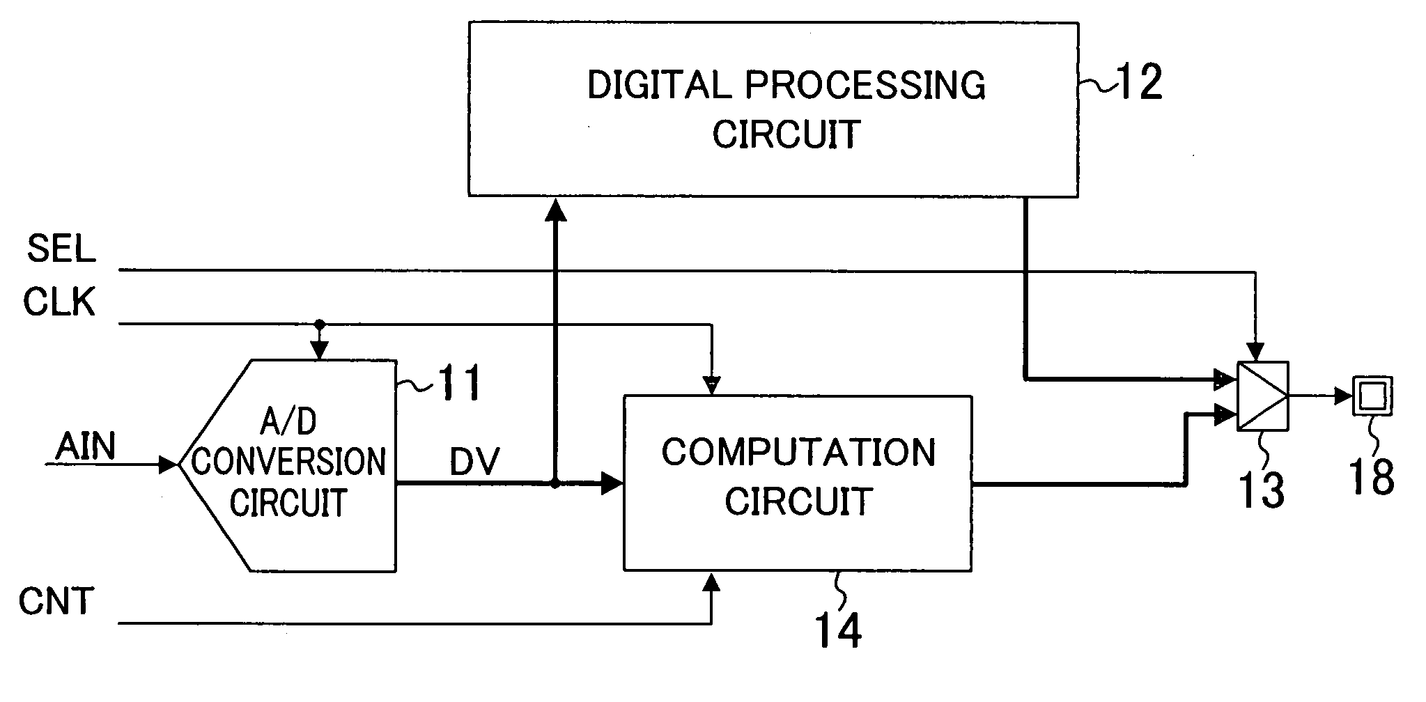
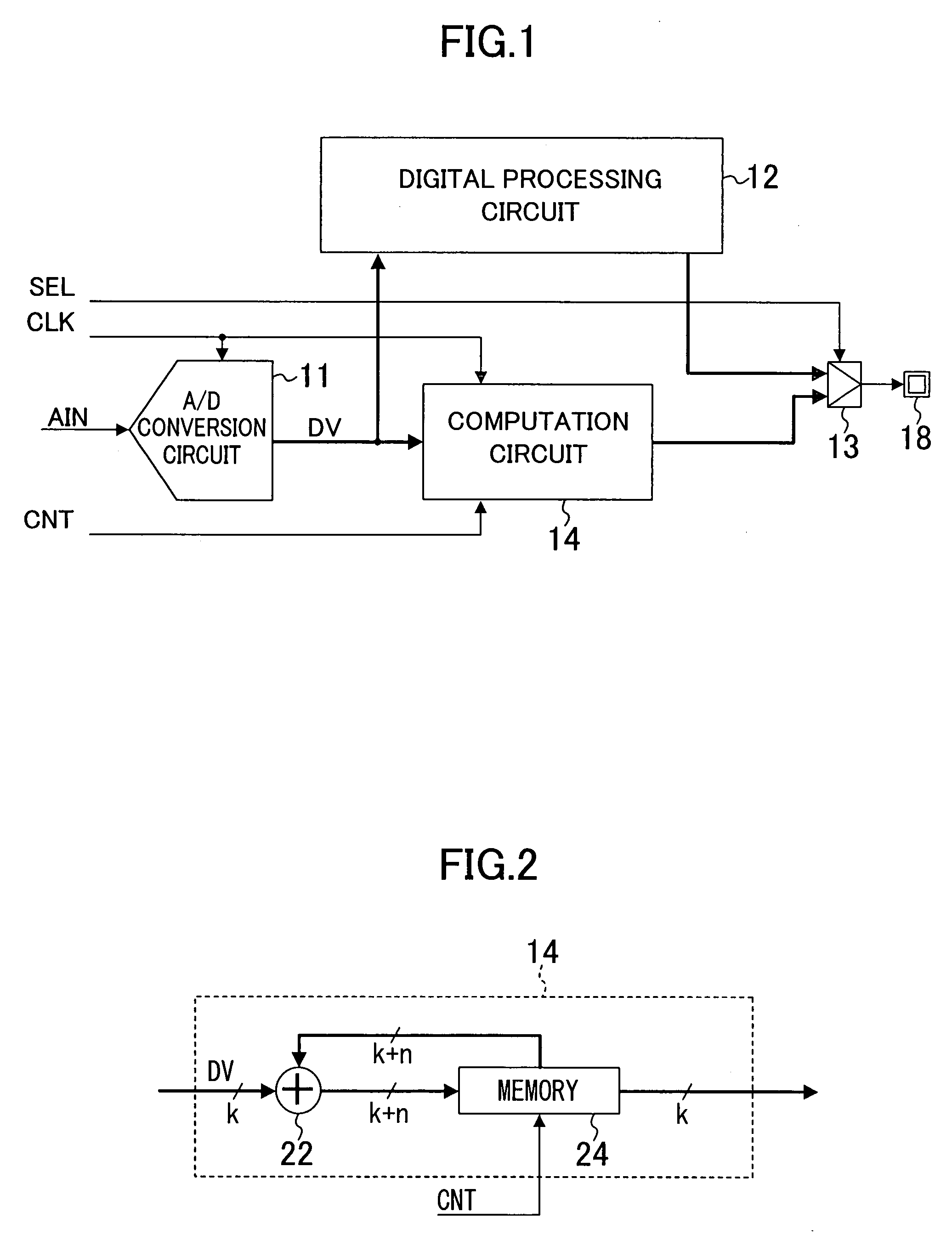
[0019]FIG. 1 is a block diagram of a semiconductor device of Embodiment 1 of the present invention. The semiconductor device of FIG. 1 includes an A / D conversion circuit 11, a digital processing circuit 12, a selector 13 and a computation circuit 14.

[0020]The A / D conversion circuit 11 A / D-converts an analog input signal AIN every clock cycle of a clock signal CLK supplied and outputs the result (A / D conversion result) to the digital processing circuit 12 and the computation circuit 14 as a digital signal DV. The clock signal CLK, the analog input signal AIN and a computation control signal CNT may be signals received from outside the semiconductor device of FIG. 1 or internal signals.

[0021]The digital processing circuit 12, which may be a logic circuit, for example, performs predetermined processing using the A / D conversion result from the A / D conversion circuit 11, and outputs the processed result to the selector 13.

[0022]The computation circuit 14 performs computation for the A / D ...

embodiment 2

[0033]FIG. 4 is a block diagram of a testing device as a semiconductor device of Embodiment 2 of the present invention. A testing device 4 of FIG. 4 includes a computation circuit 14, a signal generator 15 and a signal reader 16. A semiconductor device 2 includes an A / D conversion circuit 11.

[0034]The signal generator 15 generates an analog input signal AIN and a clock signal CLK and outputs the generated signals to the A / D conversion circuit 11. The analog input signal AIN is similar to that described in Embodiment 1 and can be a signal as shown in FIG. 3, for example. The A / D conversion circuit 11 A / D-converts the analog input signal AIN every cycle of the clock signal CLK and outputs the conversion result to the computation circuit 14 as a digital signal DV.

[0035]Also, the signal generator 15 generates the clock signal CLK and a computation control signal CNT and outputs the generated signals to the computation circuit 14. The computation circuit 14 is similar to that described i...

embodiment 3

[0037]FIG. 5 is a block diagram of a semiconductor device of Embodiment 3 of the present invention. The semiconductor device of FIG. 5 includes an A / D conversion circuit 11 and a computation circuit 30. The computation circuit 30 includes an initial value memory 31, a subtractor 32, a difference value distribution circuit 33, a counter section 34, a difference detection circuit 36 and an adder 37. The counter section 34 includes (2j+1) counters ( is an integer equal to or more than 2). These counters respectively correspond to difference values j, j−1, . . . . , 2, 1, 0, −1, −2, . . . , −j that can be outputted from the subtractor 32. The initial value memory 31 and all the counters in the counter section 34 are reset with a computation control signal CNT every time A / D conversion is performed m times.

[0038]FIG. 6 is a flowchart showing a flow of processing in the semiconductor device of FIG. 5. Referring to FIGS. 5 and 6, the processing in the semiconductor device of this embodimen...


PUM


Abstract

The semiconductor device of the present invention includes: an A / D conversion circuit for A / D-converting an analog input signal and outputting a resultant conversion result; and a computation circuit for performing, in synchronization with the A / D conversion circuit, computation for an updated conversion result without storing the updated conversion result every time the conversion result from the A / D conversion circuit is updated, to determine one computation result from a plurality of conversion results from the A / D conversion circuit and output the computation result.

Description

CROSS-REFERENCE TO RELATED APPLICATIONS[0001]This application claims priority under 35 U.S.C. §119 on Patent Application No. 2006-184275 filed in Japan on Jul. 4, 2006, the entire contents of which are hereby incorporated by reference.BACKGROUND OF THE INVENTION[0002]The present invention relates to a semiconductor device for testing an analog to digital (A / D) conversion circuit.[0003]In recent years, a semiconductor device called a system-on-a-chip has increasingly become the mainstream. In this type of device, an A / D conversion circuit, a digital circuit for performing processing based on the A / D conversion results and the like, for example, are placed on one chip. Some of such semiconductor devices include a mode switch circuit therein for enabling testing of only the A / D conversion circuit, among circuits in the device, so that the A / D conversion results can be directly outputted outside.[0004]However, if the influence of noise caused by electromagnetic waves originating from a ...

Claims


Application Information

Patent Timeline
IPC IPC(8): H03M1/10
CPCH03M1/0634H03M1/109H03M1/108
Inventor HIROSE, MASAYADAIO, KINYAOOSAKA, TETSUYANOBEKAWA, TOMOKO
Owner SOCIONEXT INC
Why Eureka
Try Eureka