Semiconductor device
a technology of magnetocoupler and power device, which is applied in the direction of magnetocoupler devices, electrical appliances, transistors, etc., can solve the problem of not considering the latch-up phenomenon, and achieve the effect of improving the latch-up immunity of the parasitic thyristor, reducing the turn-off time, and increasing the driving current quantity
- Summary
- Abstract
- Description
- Claims
- Application Information
AI Technical Summary
Benefits of technology
Problems solved by technology
Method used
Image
Examples
first embodiment
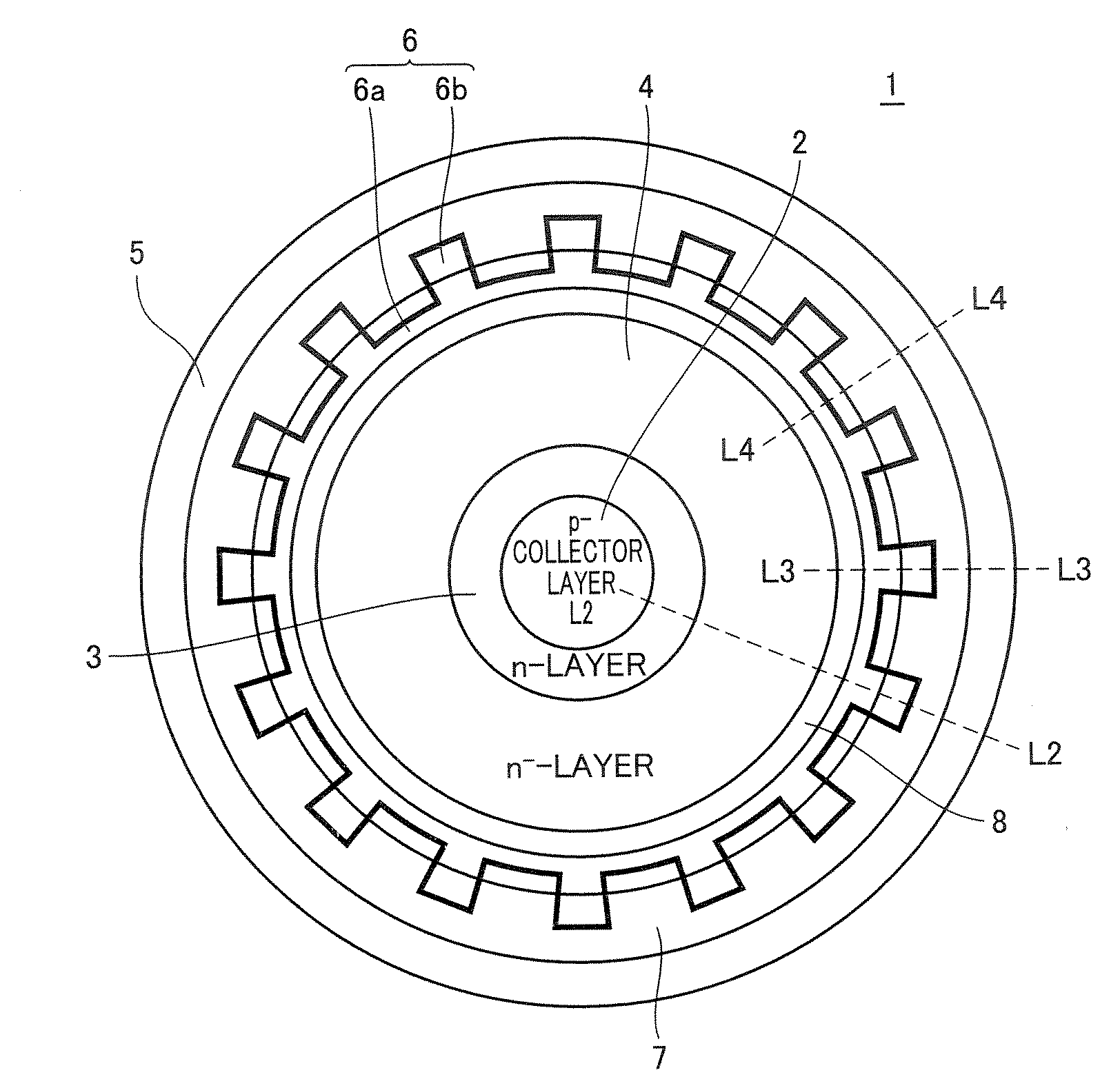
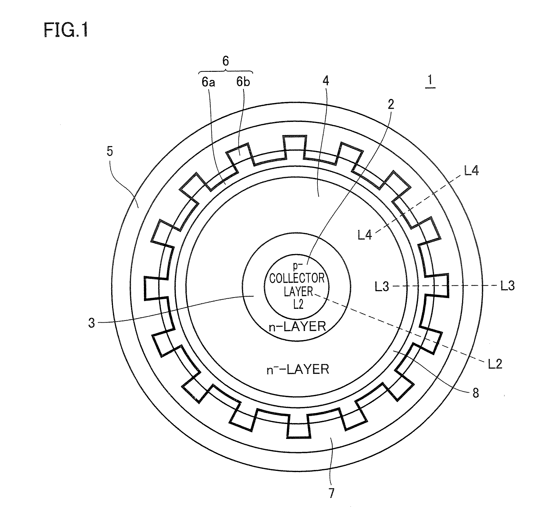
[0069]FIG. 1 schematically shows a planar layout of a lateral n-channel IGBT according to a first embodiment of the invention. FIG. 1 does not show insulating films, interconnection lines, electrodes and the like, and further does not show a heavily doped semiconductor region which is one of characteristic features of the invention.
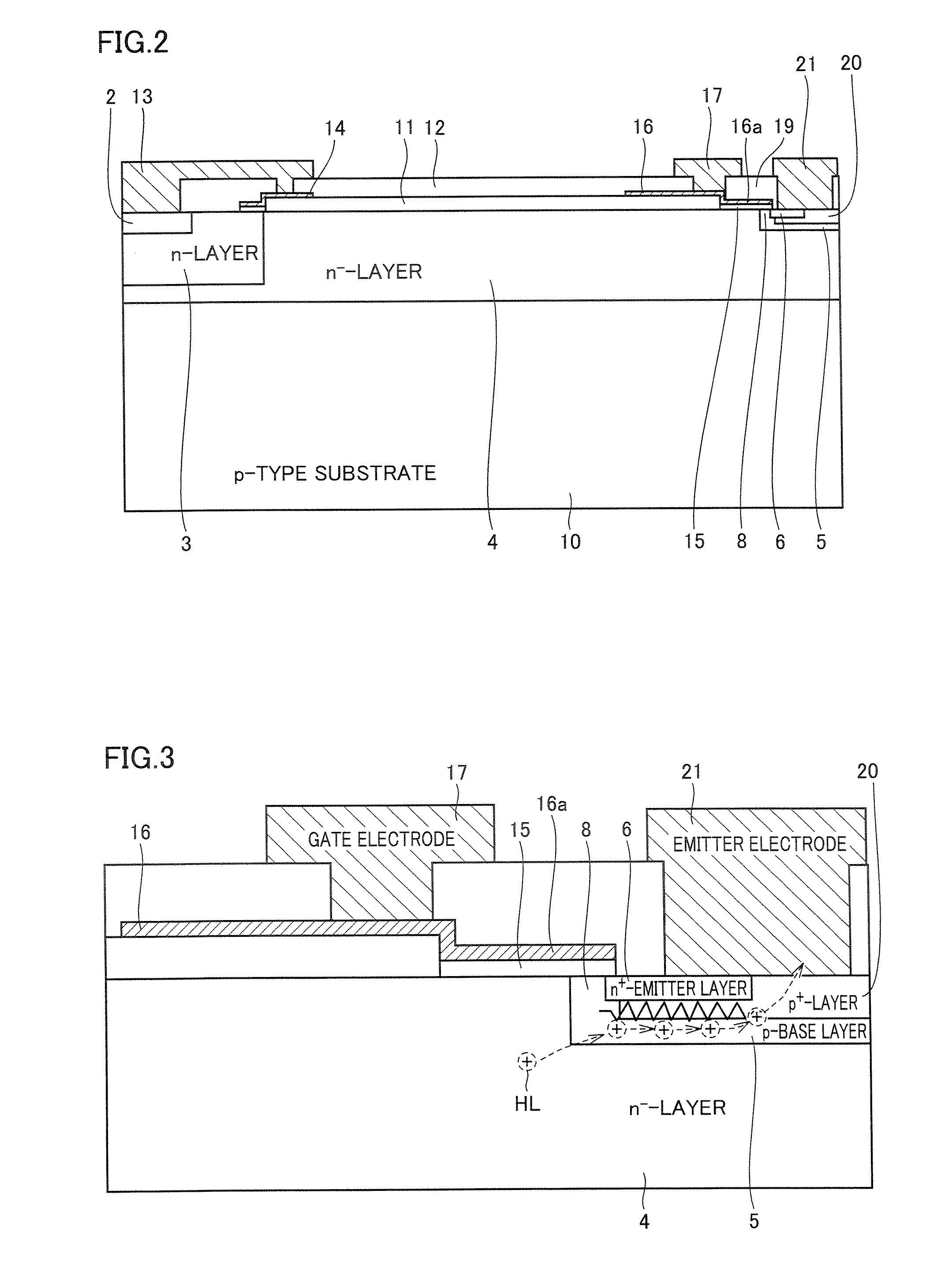
[0070]In FIG. 1, an IGBT 1 includes a p-type collector layer (first semiconductor layer region) 2 formed at a central portion in a circular form, an n-type buffer layer (semiconductor region) 3 formed surrounding collector layer 2, an n−-type drift layer (semiconductor region) 4 formed in a ring-shaped form outside buffer layer 3, an annular p-type base layer (second semiconductor region) 5 formed in a ring-shaped form outside n−-type drift layer 4, and an n+-emitter layer (third semiconductor region) 6 formed in p-type base layer 5.
[0071]Emitter layer 6 includes a main body 6a formed into a continuous, ring-shaped form and convex portions 6b that are arr...
second embodiment
[0117]FIG. 16 schematically shows a planar layout of an IGBT according to a second embodiment of the invention. For the sake of simplicity, FIG. 16 does not show the insulating films, electrode interconnection lines and heavily doped p-type layer in the base layer, similarly to FIG. 1.
[0118]The planar layout shown in FIG. 16 differs from that of the IGBT according to the first embodiment shown in FIG. 1 in the following points. As an n+-emitter layer arranged in p-type base layer, unit emitter layers (unit regions) 60 are arranged in p-type base layer 5 at predetermined circumferential intervals. Other arrangements in the planar layout of the IGBT shown in FIG. 16 are the same as those in the planar layout shown in FIG. 1. Corresponding portions are allotted with the same reference numerals, and description thereof is not repeated.
[0119]A width a of unit emitter layer 60 along circumferential direction is larger than a distance b between adjacent unit regions. Unit emitter layer 60 ...
third embodiment
[0147]FIG. 25 schematically shows a planar layout of the IGBT according to a third embodiment of the invention. For the sake of simplicity, FIG. 25 does not show the insulating films, electrodes and interconnections in the planar layout.
[0148]The planar layout shown in FIG. 25 has the same arrangement as that of the IGBT according to the first embodiment shown in FIG. 1. The IGBT shown in FIG. 25 has a cross sectional structure, in which a p+-layer is formed deeper than p-base layer 5, as will be described later in detail. N+-emitter layer 6 includes main body 6a of a ring-shaped, continuous form as well as convex portions 6b protruding in the radial direction. Other arrangements of the planar layout of the IGBT shown in FIG. 25 is the same as those of the IGBT shown in FIG. 1. Corresponding portions are allotted with the same reference numerals, and description thereof is not repeated.
[0149]FIG. 26 schematically shows a cross sectional structure taken along a line L26-L26 shown in ...
PUM
 Abstract
Description
Claims
Application Information
 - R&D
- Intellectual Property
- Life Sciences
- Materials
- Tech Scout
- Unparalleled Data Quality
- Higher Quality Content
- 60% Fewer Hallucinations
Browse by: Latest US Patents, China's latest patents, Technical Efficacy Thesaurus, Application Domain, Technology Topic, Popular Technical Reports.
© 2025 PatSnap. All rights reserved.Legal|Privacy policy|Modern Slavery Act Transparency Statement|Sitemap|About US| Contact US: help@patsnap.com


