
Optical method to monitor nano thin-film surface structure and thickness thereof

a technology of optical monitoring and nano thin films, applied in the direction of vacuum evaporation coatings, chemical vapor deposition coatings, coatings, etc., can solve the problems of inability to control the thin film structure and thickness in the deposition manufacturing process immediately, high roughness of nanocrystalline thin films made by vapor deposition, and high roughness of nanocrystalline thin films

Inactive Publication Date: 2007-12-06
GRACE SEMICON MFG CORP
View PDF2 Cites 13 Cited by
  • Summary
  • Abstract
  • Description
  • Claims
  • Application Information

AI Technical Summary

Benefits of technology

[0008]An object of the present invention is to provide an optical method to monitor a nano thin-film deposition manufacturing process, which simulates the transmittance, reflectance and other optical parameters of a nanocrystalline thin film in the deposition manufacturing process to analyze the structure of the nano thin film, and thus achieves the goal of monitoring the thin-film deposition manufacturing process.
[0010]Further another objective of the present invention is to provide an optical mode simulating nanocrystalline structures, which precisely monitors the surface structure and thickness of a nanocrystalline thin film.

Problems solved by technology

Therefore, using the classical theory to predict the physical behavior in such a small scale is not proper.
However, a nanocrystalline thin film made by vapor deposition has high roughness, a low volume fraction in the surface specific structure, and a high dense bottom layer.
Because this double-layer structure in the thin film manufacturing cannot decide the thin film structure and thickness by non-touch methods, such as the quartz oscillating frequency, split-beam spectrum and polarization ellipse.
However, this method cannot control the thin film structure and thickness in the deposition manufacturing process immediately.
Hence, the quality of the nanocrystalline thin film cannot be controlled, and the failure ratio rises correspondingly.

Method used


Image

  • Optical method to monitor nano thin-film surface structure and thickness thereof
  • Optical method to monitor nano thin-film surface structure and thickness thereof
  • Optical method to monitor nano thin-film surface structure and thickness thereof

Examples


Embodiment Construction

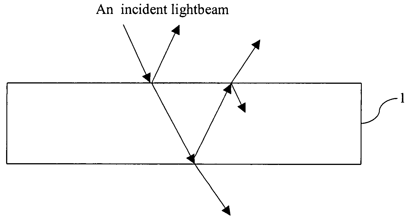
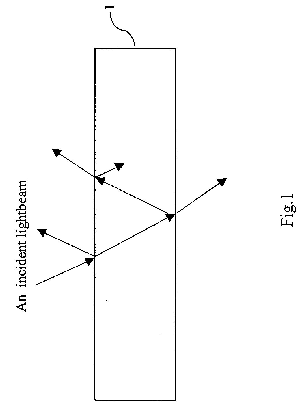
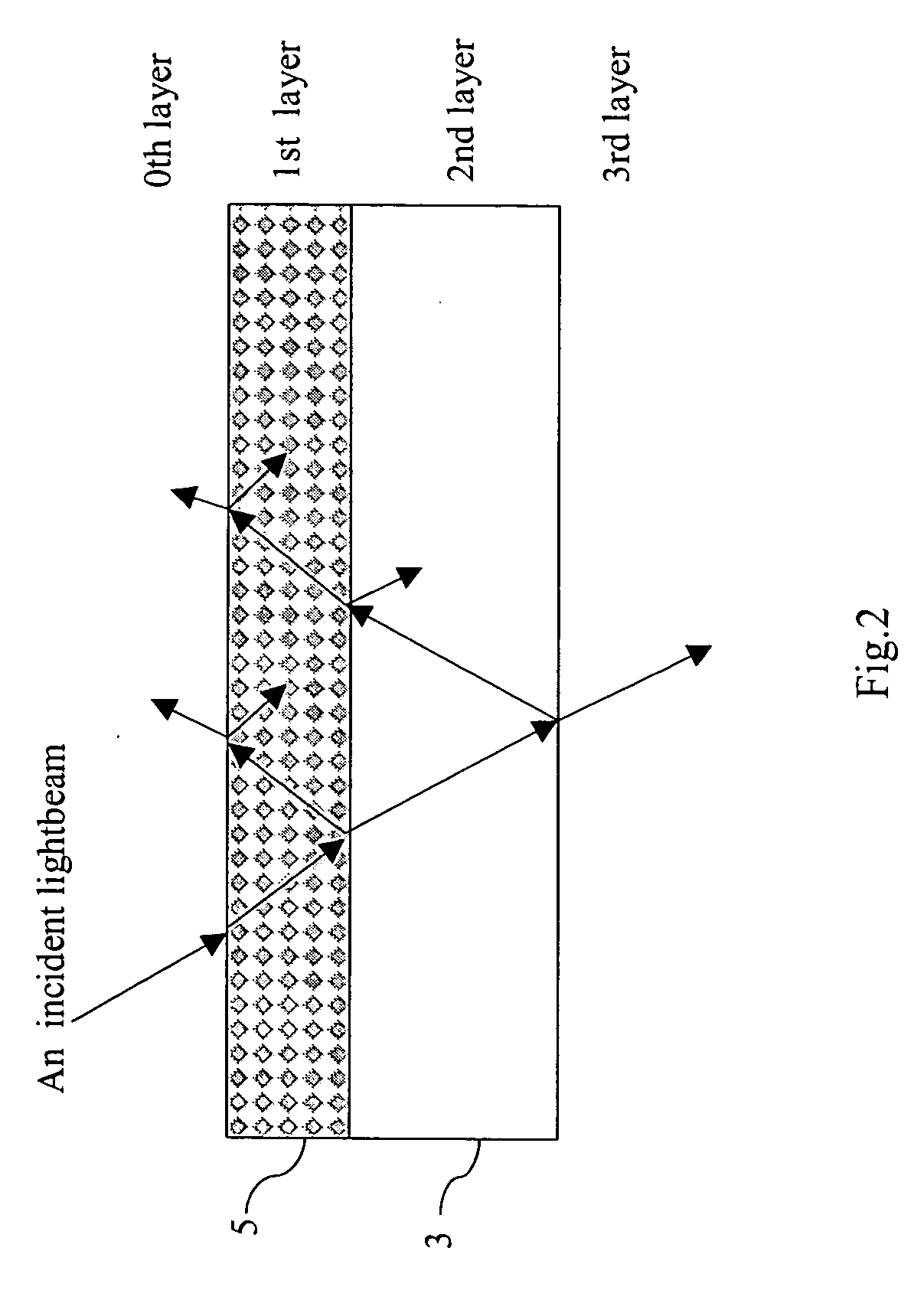
[0026]This invention presents a method to detect a thin-film surface structure and the thickness thereof. Specifically, this invention is to monitor nanocrystalline thin films, wherein the light characteristics such as transmission, reflection, refraction, absorption and so forth, are applied to detect the structure and thickness of thin films.

[0027]As for a structure, a nanocrystalline thin film is not a homogeneous single-layer structure, but is a nonhomogeneous single-layer one comprising a dense bottom layer and a high roughness surface structure. If the dense bottom layer and surface structure are taken into account, a nanocrystalline thin film is a nonhomogeneous double-layer structure comprising a low dielectric constant layer with the low volume fraction surface reducing the refractive index and a dense bottom layer with high refractive index. Therefore, utilize the inherent structure of a nano thin film to calculate the thin-film transmittance and the possible convergence r...


PUM

PropertyMeasurementUnit
Thicknessaaaaaaaaaa
Surfaceaaaaaaaaaa
Transparencyaaaaaaaaaa

Abstract

A method to monitor a nanocrystalline film surface structure and the thickness thereof uses the surface structure characteristics of the vapor deposition nanocrystalline thin films having the low volume fraction to make a nanocrystalline thin film become a nonhomogeneous double-layer structure comprising a dense bottom layer having high index of refraction and a surface layer having the low volume fraction. The optical module of this double-layer structure can be used to simulate the characteristics of the nanocrystalline structure. That is to say, in the thin film deposition manufacturing process, if the thin film structure satisfies the optical module of the double-layer structure, this means it has the nanocrystalline characteristic. Hence, in the manufacturing process, use the optical instruments to measure the thin film and the substrate and to calculate the optical parameters; thus a nanocrystalline film surface structure and the thickness thereof can be precisely monitored immediately.

Description

BACKGROUND OF THE INVENTION[0001]1. Field of the Invention[0002]This invention relates to an optical application method, and more particularly to an optical method to monitor a nano thin-film surface structure and the thickness thereof in the nano thin-film deposition manufacturing process.[0003]2. Description of the Prior Art[0004]Nanotechnology has become a very popular topic recently, and it is even considered as one of the most essential technology that has a significant influence on human's future. Nanometer is an adjective of size. The size of nano structures is about 1˜100 nanometers which are between molecule and submicron scale. Therefore, using the classical theory to predict the physical behavior in such a small scale is not proper. The influence of quantum effects will be a non-neglected factor, and further the proportion of the surface area increases a lot. So the physical, chemical and biological properties in such a small scale will be very different from those in a l...

Claims


Application Information

Patent Timeline
IPC IPC(8): C23C16/52
CPCC23C16/52C23C14/54
Inventor HUANG, CHENG-CHIA
Owner GRACE SEMICON MFG CORP
Learn More