Wafer-level method for thinning imaging sensors for backside illumination
a technology of imaging sensors and wafers, applied in semiconductor devices, diodes, electrical devices, etc., can solve the problems of inability to handle thin wafers after, inability to thinning wafers, and inability to achieve the effect of reducing the thickness of the carrier,
- Summary
- Abstract
- Description
- Claims
- Application Information
AI Technical Summary
Problems solved by technology
Method used
Image

Examples
Embodiment Construction
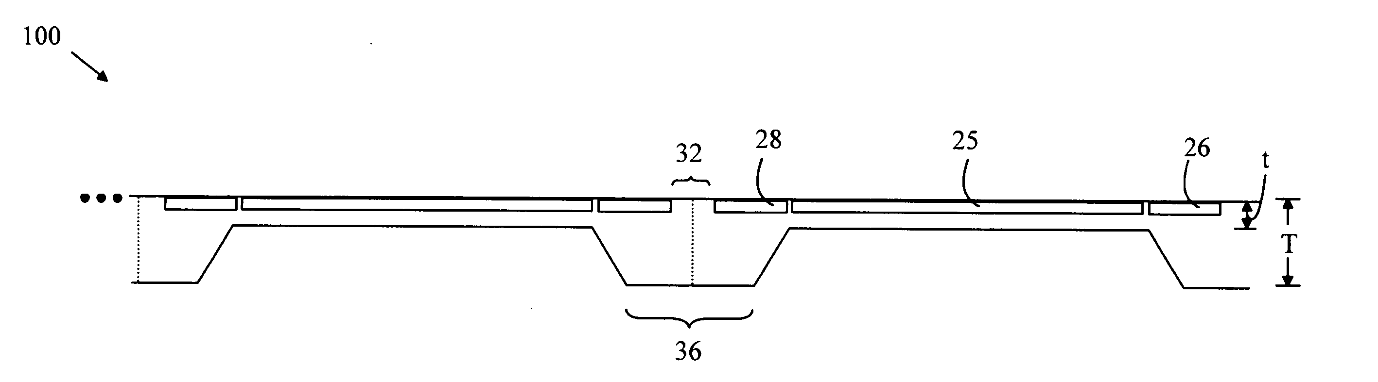
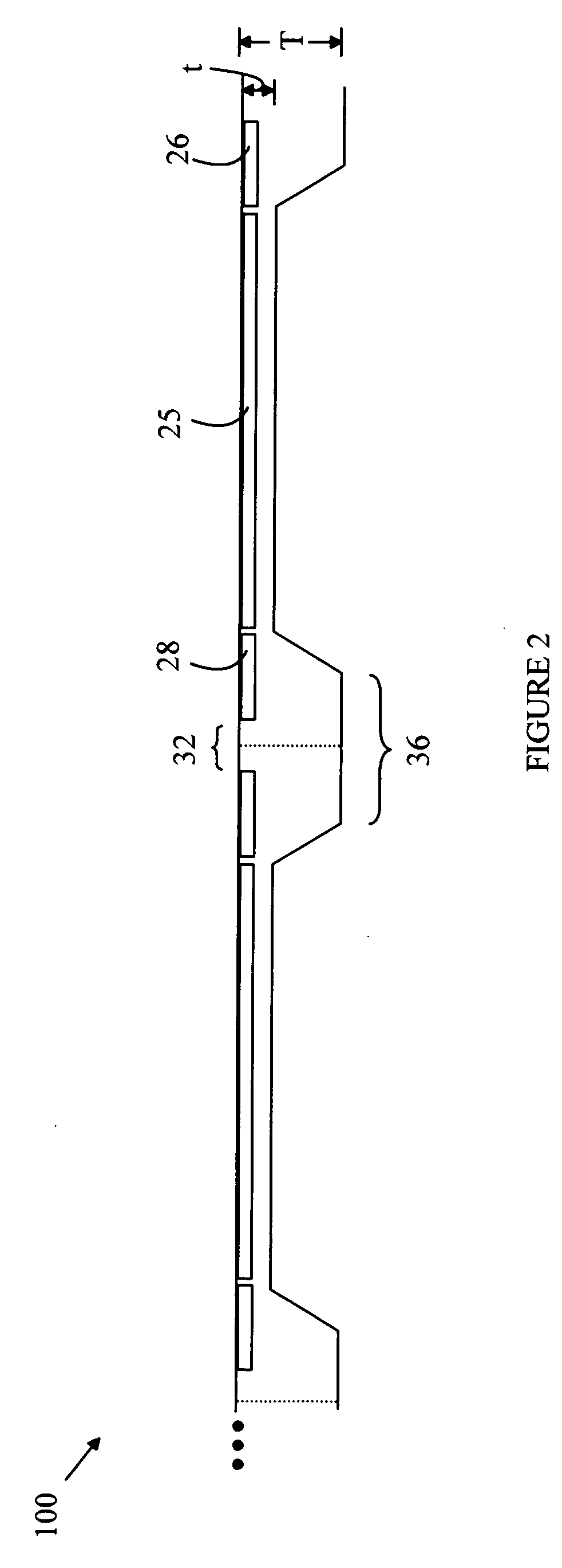
[0011] The present invention is based on the observation that each imaging chip includes a peripheral region that is used for scribe lanes and circuitry other than the circuitry involved in the pixel-by-pixel charge conversion. When the wafer is thinned, these regions are left unthinned and provide a ribbed structure that provides sufficient strength to allow the thinned wafer to be handled and finally diced. Hence, all the imager chips can be thinned at the wafer level simultaneously, which provides a significant cost advantage.
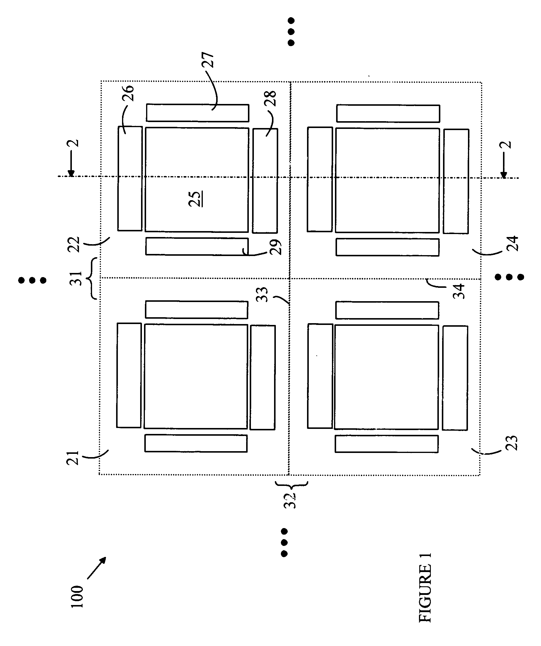
[0012] Refer now to FIG. 1, which illustrates a portion of a wafer 100 containing CCD chips of a typical construction after the circuitry on the front side of the wafer has been fabricated. FIG. 1 is a top view of wafer 100. Four CCD chips are shown in FIG. 1 at 21-24. Each chip includes an optical sensing area 25 and support circuitry 26-29 that is constructed in the regions around optical sensing area 25. Optical sensing area 25 is typically a two-dimensi...
PUM
 Abstract
Description
Claims
Application Information
 - R&D
- Intellectual Property
- Life Sciences
- Materials
- Tech Scout
- Unparalleled Data Quality
- Higher Quality Content
- 60% Fewer Hallucinations
Browse by: Latest US Patents, China's latest patents, Technical Efficacy Thesaurus, Application Domain, Technology Topic, Popular Technical Reports.
© 2025 PatSnap. All rights reserved.Legal|Privacy policy|Modern Slavery Act Transparency Statement|Sitemap|About US| Contact US: help@patsnap.com