
Method of manufacturing wiring substrate, and liquid ejection head manufactured by same

a technology of wiring substrate and liquid ejection head, which is applied in the direction of printing, lithographic mask, inking apparatus, etc., can solve the problems of weak adhesive characteristics, functional problems, and the inability to meet the requirements of the substrate, so as to achieve good heat dissipation, good adhesion, and easy formation of high-density electrical wires

Inactive Publication Date: 2007-09-27
FUJIFILM CORP
View PDF6 Cites 3 Cited by
  • Summary
  • Abstract
  • Description
  • Claims
  • Application Information

AI Technical Summary

Benefits of technology

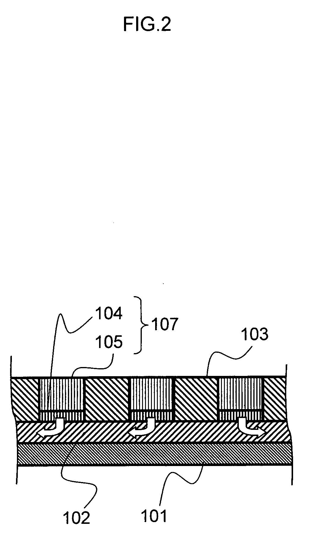
[0010]The present invention has been contrived in view of the foregoing circumstances, an object thereof being to provide a method of readily forming high-density electrical wires having high heat radiating properties and strong adhesion to the substrate, and to provide a liquid ejection head manufactured by means of this method.
[0021]The present invention is beneficial in that it is possible to readily form high-density electrical wires having good heat radiating properties and good adhesion with respect to the substrate. Moreover, a liquid ejection head can be made more compact in size by using a circuit substrate manufactured according to the present invention.

Problems solved by technology

Therefore, there is a possibility of declining the adherence between the electrical wires and the substrate, that is to say, close-contact characteristics therebetween.
In this method, the contact section between an electrical wire and the substrate is formed on one surface only, and therefore, the finer the electrical wires, the weaker the adhesive characteristics tend to become.
In particular, if there is a vibration generating section or operating section on or near the substrate, then the electrical wires may become detached from the substrate due to vibrations caused by the vibrating section or operating section, and this may lead to functional problems.
However, the film obtained by this substitution plating has a coarse crystal structure, a large number of pinholes, and poor adhesive characteristics.
Moreover, normally, zinc oxide is used as a transparent conductive material, and it has poor insulating properties.
Hence, there is a possibility that, if electrical wires are formed on a zinc oxide film, then the current that should flow inside an electrical wire flows into the adjacent electrical wires through the zinc oxide film, and insulation is not achieved between the electrical wires, and consequently the wiring substrate ceases to function correctly.
In cases where the zinc oxide is doped with an alkali metal, the resistance tends to decline yet further and this possibility becomes more serious.

Method used


Image

  • Method of manufacturing wiring substrate, and liquid ejection head manufactured by same
  • Method of manufacturing wiring substrate, and liquid ejection head manufactured by same
  • Method of manufacturing wiring substrate, and liquid ejection head manufactured by same

Examples


first embodiment

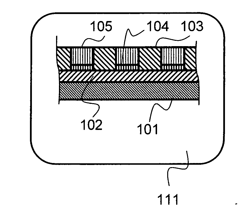
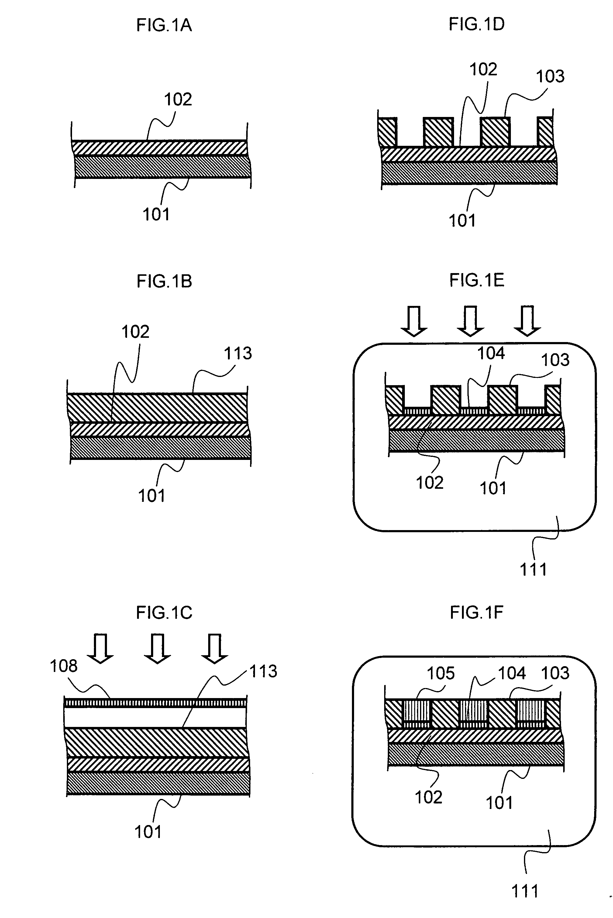
[0032]FIGS. 1A to 1F are diagrams showing a method of manufacturing a wiring substrate according to a first embodiment of the present invention. The first embodiment relates to a method of manufacturing a wiring substrate by means of photolithography.

[0033]As shown in FIG. 1A, a photocatalyst containing layer 102 is formed on a substrate 101 made of an insulator material.

[0034]The substrate 101 is formed of a glass substrate, a silicon wafer, a resin substrate, a ceramic substrate, or the like. The photocatalyst containing layer 102 contains a photocatalytic material which displays photocatalytic activity when irradiated with ultraviolet light. In the present embodiment, the photocatalytic material is required to meet some conditions, as described below with reference to FIG. 7.

[0035]It is necessary that the photocatalytic material used in the present embodiment should be capable of directly reducing the target metal material.

[0036]The reduction potential (in the reduction of a copp...

second embodiment

[0061]FIGS. 6A to 6F are diagrams showing a method of manufacturing a wiring substrate according to a second embodiment of the present invention. The second embodiment relates to a method in which a wiring substrate is manufactured by imprinting.

[0062]As shown in FIG. 6A, a photocatalyst containing layer 102 is formed on a substrate 101 made of an insulator material.

[0063]The substrate 101 is made of a glass substrate, a silicon wafer, a resin substrate, a ceramic substrate, or the like. The photocatalyst containing layer 102 contains a photocatalytic material which displays photocatalytic activity when irradiated with ultraviolet light. In the present embodiment, the photocatalytic material is required to meet some conditions, as described below with reference to FIG. 7.

[0064]More specifically, it is necessary that the photocatalytic material used in the present embodiment should be capable of directly reducing the target metal material.

[0065]The reduction potential (in the reducti...


PUM


Abstract

The method of manufacturing a wiring substrate includes the steps of: forming a photocatalyst containing layer which is made of a material containing a photocatalytic material, on a substrate made of an insulating material; forming a resin layer in regions other than wire regions on the photocatalyst containing layer; radiating ultraviolet light on the photocatalyst containing layer while the substrate provided with the resin layer and the photocatalyst containing layer is immersed in a solution containing at least a metal ion and a sacrificial reagent, in such a manner that metal is deposited on exposed regions of the photocatalyst containing layer.

Description

BACKGROUND OF THE INVENTION[0001]1. Field of the Invention[0002]The present invention relates to a method of manufacturing a wiring substrate and to a liquid ejection head manufactured according to this method, and more particularly, it relates to a method of manufacturing a fine wiring substrate having good adhesive properties and to a liquid ejection head manufactured according to this method.[0003]2. Description of the Related Art[0004]In recent years, there has been a tendency for the various electronic components which are used in an electronic device to be integrated at higher density, in accordance with reductions in the weight and size of these electronic devices. In response to this, the electrical wiring patterns of the wiring substrate with which various electronic components are mounted are formed to become higher density, and the line width of the electrical wirings or the interval between the wirings is required to have very fine dimensions of the order of approximatel...

Claims


Application Information

Patent Timeline
IPC IPC(8): H01L23/52H01L23/48H01L29/40
CPCB41J2/14233B41J2/161B41J2/1643B41J2/1645B41J2002/14491B41J2202/18H01L21/4846H01L2924/0002H05K3/184H05K3/185H05K2203/0551H01L2924/00
Inventor OHTA, HIROSHI
Owner FUJIFILM CORP
Learn More