Circuit board and manufacturing method thereof, electro-optical device, and electronic apparatus
a manufacturing method and circuit board technology, applied in the field of circuit board, can solve the problems of large off-current, inability to miniaturize the element, and inability to achieve excellent performance of organic transistors, and achieve the effect of high performan
- Summary
- Abstract
- Description
- Claims
- Application Information
AI Technical Summary
Benefits of technology
Problems solved by technology
Method used
Image

Examples
first embodiment
[0050]First, a circuit board according to a first embodiment of the invention will now be described.
(1) Circuit Board
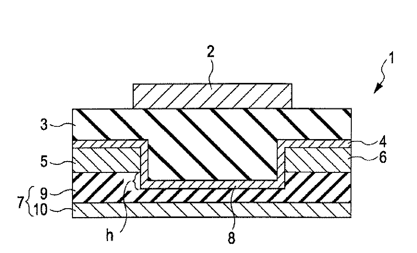
[0051]FIG. 1 is a schematic longitudinal sectional view of a circuit board 1 according to an embodiment of the invention. Hereinafter, an upper side in FIG. 1 is referred to as up, and a lower side in FIG. 1 is referred to as down.
[0052]The circuit board 1 shown in FIG. 1 includes a gate electrode 2, a gate insulating layer 3, an organic semiconductor layer 4, a source electrode 5, a drain electrode 6, a substrate 7, and a recessed portion 8, and has a top-gate / bottom-contact type structure.
[0053]Hereinafter, structures of the components will be described one after another.
[0054]The gate electrode 2 is used for providing an electric field to the organic semiconductor layer 4. The gate electrode 2 is disposed on one side of the substrate 7 to contact the gate insulating layer 3 without contacting the source electrode 5 and the drain electrode 6.
[0055]The material of th...
second embodiment
[0111]A circuit board 1 and a manufacturing method thereof according to a second embodiment of the invention will now be described with focusing on differences from the first embodiment, and description about common features is omitted.
(1) Circuit Board
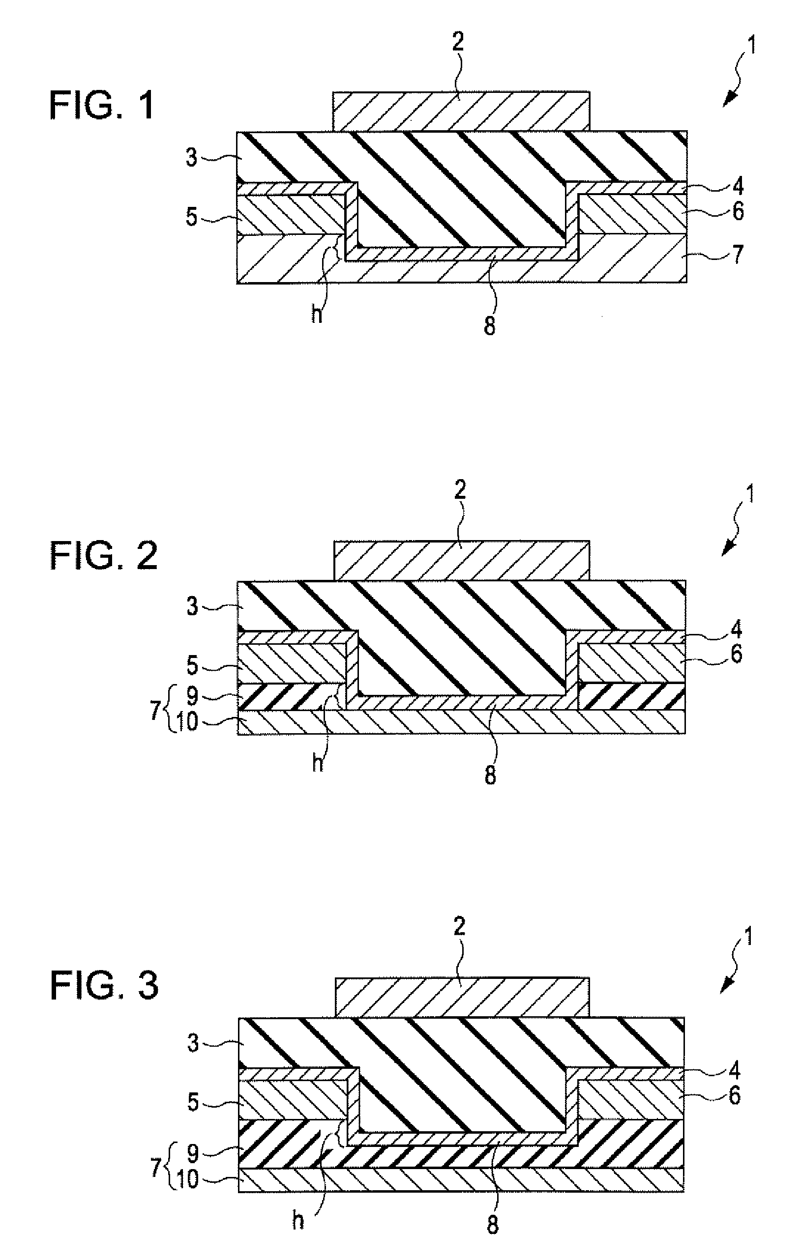
[0112]FIG. 2 is a schematic longitudinal sectional view of a circuit board 1 according to another embodiment of the invention. Hereinafter, an upper side in FIG. 2 is referred to as up, and a lower side in FIG. 2 is referred to as down.
[0113]The circuit board 1 shown in FIG. 2 has a same structure as that of the circuit board 1 in the first embodiment except the existence of a base insulating layer 9.
[0114]In other words, there are differences in the second embodiment from the first embodiment that a base insulating layer 9 is formed and the whole part of the base insulating layer 9 disposed between the source electrode 5 and the drain electrode 6 is etched.
[0115]The base insulating layer 9 and a base body 10 construct the substrate 7...
third embodiment
[0140]A circuit board 1 and a manufacturing method thereof according to a third embodiment of the invention will now be described with focusing on differences from the first and second embodiments and description about common features is omitted.
(1) Circuit Board
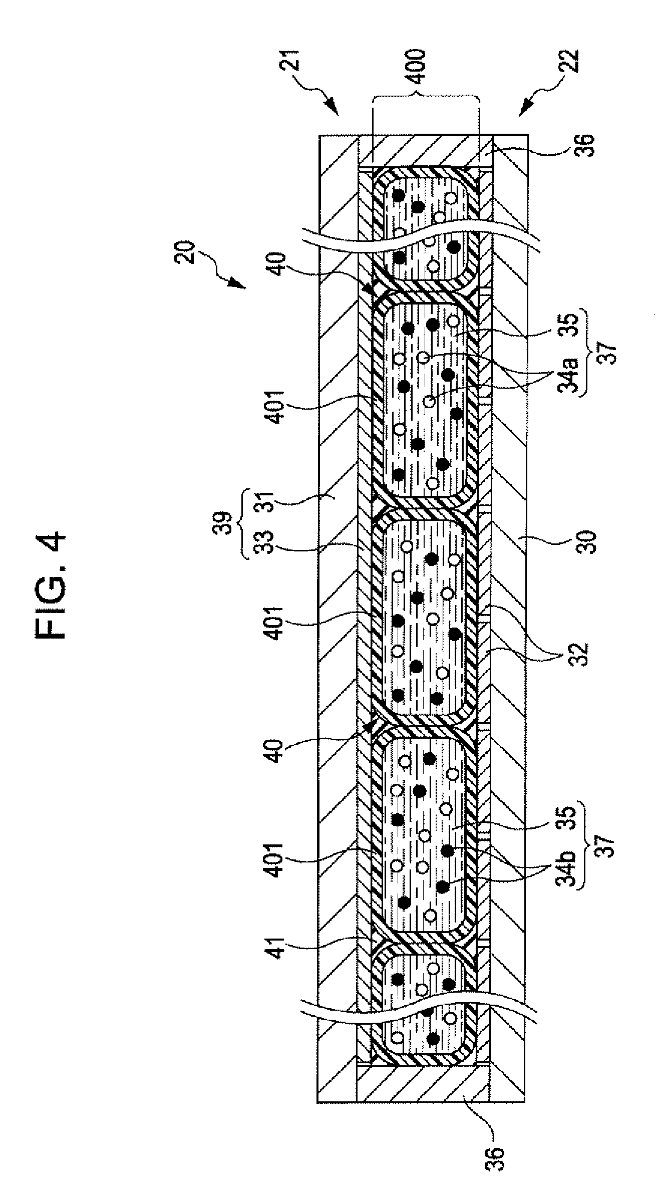
[0141]FIG. 3 is a schematic longitudinal sectional view of a circuit board 1 according to another embodiment of the invention. Hereinafter, an upper side in FIG. 3 is referred to as up, and a lower side in FIG. 3 is referred to as down.
[0142]The circuit board 1 shown in FIG. 3 has the same structure as that of the circuit board 1 in the second embodiment except an etching status of a base insulating layer 9.
[0143]In other words, the circuit board 1 of the third embodiment has a difference from that of the second embodiment in that a part of a region of the base insulating layer 9 interposed between a source electrode 5 and a drain electrode 6 is etched.
(2) Method of Manufacturing Circuit Board
[0144]The circuit board 1 descri...
PUM
 Abstract
Description
Claims
Application Information
 - R&D
- Intellectual Property
- Life Sciences
- Materials
- Tech Scout
- Unparalleled Data Quality
- Higher Quality Content
- 60% Fewer Hallucinations
Browse by: Latest US Patents, China's latest patents, Technical Efficacy Thesaurus, Application Domain, Technology Topic, Popular Technical Reports.
© 2025 PatSnap. All rights reserved.Legal|Privacy policy|Modern Slavery Act Transparency Statement|Sitemap|About US| Contact US: help@patsnap.com