Antenna Assembly and Multibeam Antenna Assembly
- Summary
- Abstract
- Description
- Claims
- Application Information
AI Technical Summary
Benefits of technology
Problems solved by technology
Method used
Image
Examples
first embodiment
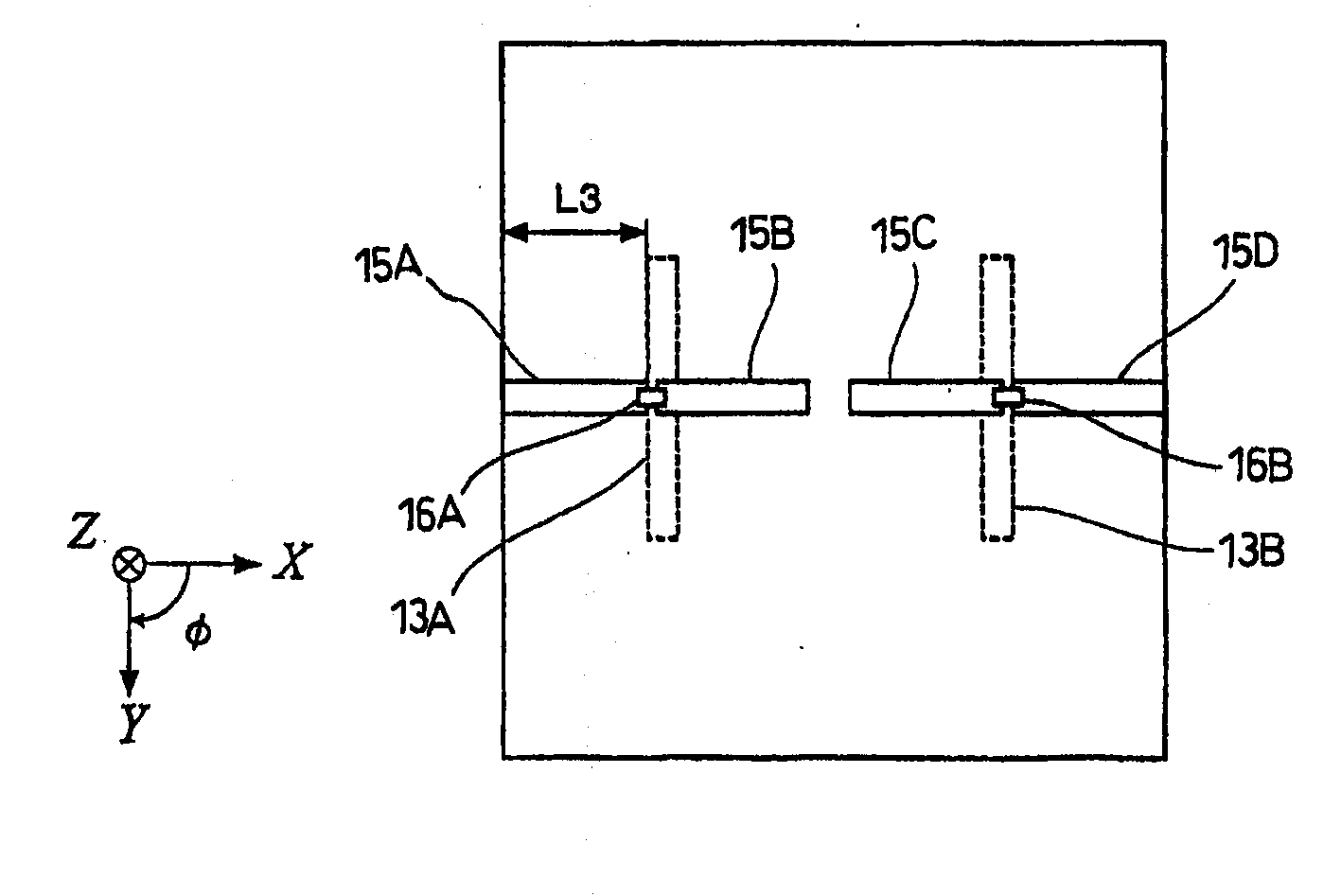
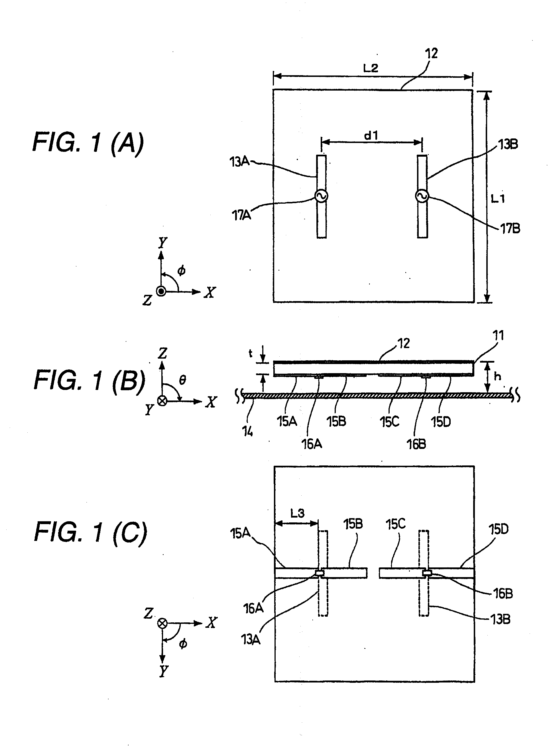
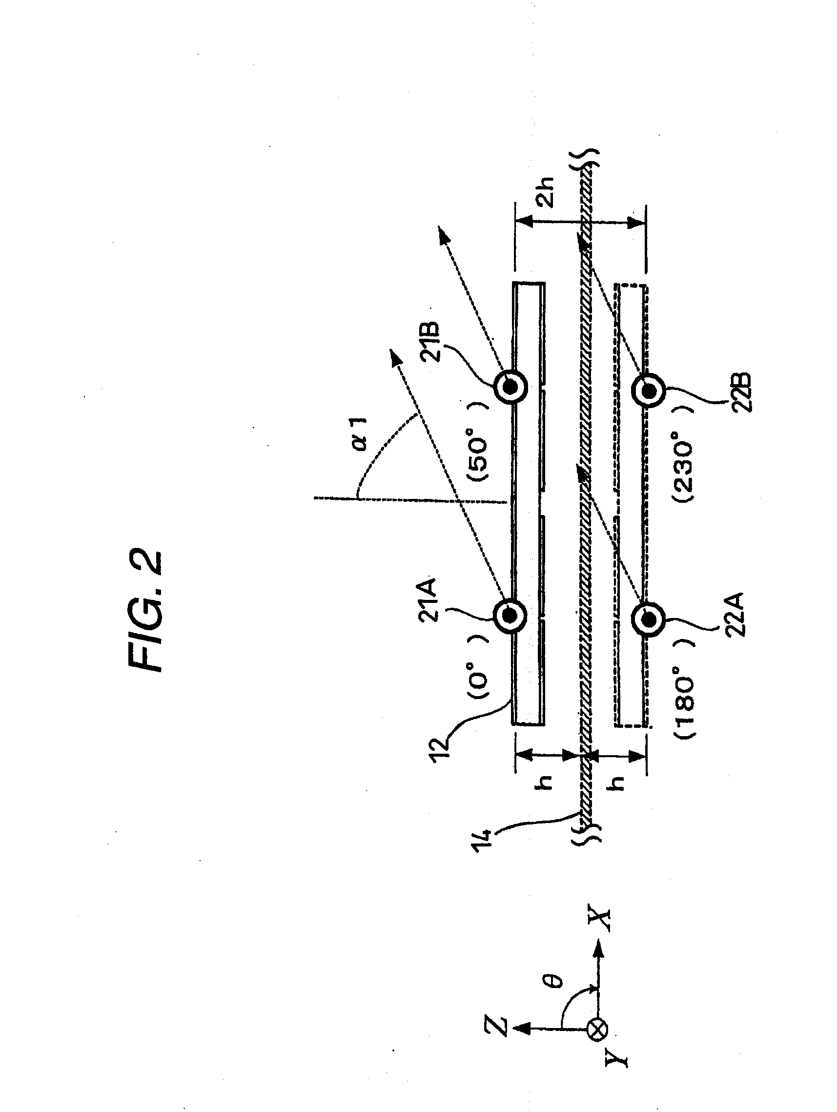
[0045]FIG. 1 shows a constitution of an antenna device according to a first embodiment of the invention. This antenna device includes a substrate 11 made of a dielectric material, a copper foil layer 12, slot elements 13A and 13B, a reflecting plate 14, parasitic elements 15A to 15D, switching elements 16A and 16B, and feeding portions 17A and 17B. Here, this embodiment is described for an antenna operating frequency of 5 GHz.
[0046] The substrate 11 has a specific dielectric constant ∈r of 2.6, a thickness t of 8 mm (or 0.21 wavelength (i.e., an effective wavelength in a dielectric)), and sizes L1×L2 of 44 mm×46 mm (or 0.73 wavelength×0.77 wavelength), for example.
[0047] The copper foil layer 12 is made of a copper foil adhered to the +Z side face of the substrate 11.
[0048] The slot elements 13A and 13B are formed into such cavities by cutting the copper foil layer 12 as have a length of 18.5 mm (or about 0.5 wavelength) and a width of 1 mm. The slot elements 13A and 13B are arra...
second embodiment
[0074] Next, an antenna device according to a second embodiment of the invention is described in detail with reference to the accompanying drawings. In this embodiment, however, the same portions as those of the first embodiment shown in FIG. 1 are omitted in their detail description by designating them by the common reference numerals. Here, the description is also made in this embodiment by assuming that the operating frequency of the antenna is 5 GHz.
[0075]FIG. 6 shows a constitution of the antenna device according to the second embodiment of the invention. This antenna device is equipped with not only the slot elements 13A and 13B but also slot elements 41A and 41B, and is constituted by arraying two sets of antenna devices of the first embodiment at right angles.
[0076] The slot elements 41A and 41B are formed into such cavities by cutting the copper foil layer 12 as have a length of 18.5 mm and a width of 1 mm. The slot elements 41A and 41B are arranged to intersect the slot ...
third embodiment
[0090] Next, an antenna device according to a third embodiment of the invention is described in detail with reference to the accompanying drawings. In this embodiment, however, the same portions as those of the first embodiment shown in FIG. 1 are omitted in their detail description by designating them by the common reference numerals. Here, the description is also made in this embodiment by assuming that the operating frequency of the antenna is 5 GHz.
[0091]FIG. 8 shows a constitution of the antenna device according to the third embodiment of the invention. Slot elements 51A to 51D, connecting conductors 52A to 52D, parasitic elements 15A to 15D, slot alternative elements 53A and 53B and a feeding portion 54 are included in the copper foil layer 12 of the substrate 11.
[0092] The slot elements 51A to 51B are formed into such cavities by cutting the copper foil layer 12 as are arranged in a square shape to have an element length L4 of 16.3 mm (or about one third wavelength) and an ...
PUM
 Abstract
Description
Claims
Application Information
 - R&D
- Intellectual Property
- Life Sciences
- Materials
- Tech Scout
- Unparalleled Data Quality
- Higher Quality Content
- 60% Fewer Hallucinations
Browse by: Latest US Patents, China's latest patents, Technical Efficacy Thesaurus, Application Domain, Technology Topic, Popular Technical Reports.
© 2025 PatSnap. All rights reserved.Legal|Privacy policy|Modern Slavery Act Transparency Statement|Sitemap|About US| Contact US: help@patsnap.com


